Dear friends, are you still troubled by the frequent return of PCB orders? As an engineer who has been working in PCB manufacturing industry for many years, I know the reason behind this trouble. Orders are usually returned because of technical problems such as design specification discrepancies, file format errors, missing key parameters, etc. Today, let me take you in-depth understanding of the specific aspects of PCB engineering review, by understanding the key points of the engineering review, you will be able to prevent common problems in advance, and establish smoother communication with the manufacturer.
Why Is an Engineering Review Needed?
Before we get into the details, you may ask: Why do we need such a rigorous engineering review? In fact, a rigorous engineering review not only ensures the quality of your PCB products, but also:
- Avoid downtime losses in the middle of production
- Reduce unnecessary back and forth communication
- Shorten overall lead time
- Save your valuable time and cost
Let's take a look at how ApplePCB's engineering department is the gatekeeper for your order!
Gerber File Specification Checking

Do you remember the last time you submitted an order and the engineer came to you asking ‘Where are your impedance requirements labeled?’ or ‘Can you provide the full version of the stacking table?’
To avoid similar situation, we suggest you prepare the following information when submitting your order:
- Complete Gerber file (with all layers)
- Detailed fabrication specifications
- Stacking data sheet
- Impedance control requirements (if any)
- Detailed drilling requirements
- Surface treatment process requirements
Board Thickness Control
In many years of PCB manufacturing experience, we found that many customers have some confusion in the board thickness control, especially in the special process requirements are more likely to have problems.
1.Standard Tolerance Control
We recommend that you consider the tolerance range at the design stage to avoid rework at a later stage. Our standard process tolerance is 4 mil (1 mil = 0.0254mm). This standard applies to most conventional PCB manufacturing requirement.
2.Special Tolerance Control
If you need tighter tolerance control, please note that smaller tolerance requirement are marked. Normal plate thickness tolerance control within 10%. It should be noted that tighter tolerances may affect product cost and lead time, and it is recommended that special tolerances be required only when necessary.
3.Dry Film Thickness
If your PCB design uses 16mil dry film, then the thickness of the entire PCB board should not exceed 126mil (about 3.2mm), otherwise it may affect the manufacturing quality of the product. This is an important parameter that our engineering department will strictly control when reviewing orders. This limit exists for the following technical reasons:
- The thickness of the dry film affects the etching accuracy
- Impacts the quality of through-hole plating
- Relates to the forming ability of the line
4.Special Board Thickness Requirements
When the PCB thickness is greater than 2mm, special attention should be paid to the cross-section ratio should not exceed 1:8, this is to ensure the quality of drilling hole and product reliability.
5.Common Problems and Solutions
Problem: Why is my order being returned saying the tolerance requirements are unreasonable?
Solution:
- Check whether it is out of the standard tolerance range
- Confirm the necessity of special tolerance
- You can communicate with engineers for alternative solutions.
Problems : Why are there special requirements for boards larger than 2mm?
Solution:
- Consider using a multi-layer lamination solution
- Pay attention to the drilling ratio requirement
- Discuss feasibility with engineers in advance
Material Selection Points
1.Material Certification and Compatibility
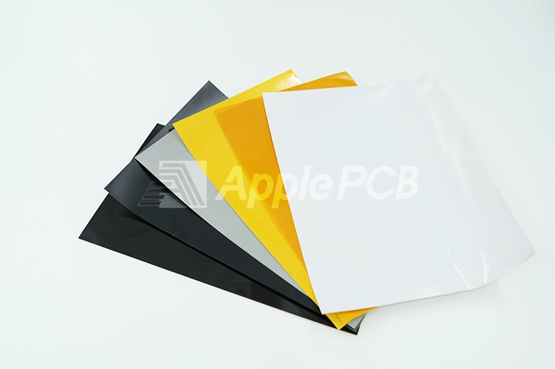
If your project requires UL certification, please clearly mark whether the material must be UL certified when placing an order. This will help us to choose the right certified material for you.
It is recommended that you prioritize the material type commonly used by PCB manufacturers, which not only shortens the delivery time, but also ensures more stable quality and more favorable prices. If you specify a material that is not commonly used, it does not matter, we have a wealth of board resources, our engineers will also suggest alternatives for your reference.
2.Material Performance Parameters
When selecting PCB materials, please pay special attention to whether the following key parameters meet your design requirements:
- Glass transition temperature (Tg)
- Decomposition temperature (Td)
- Dielectric constant (Dk)
- Loss factor (Df)
- Z-axis coefficient of thermal expansion (Z-CTE)
- Temperature resistance (T300/T288/T260)
- Comparative leakage current (CTI)
- CAF resistance
3.Special Requirement Tips
For high Tg materials (≥170℃), we recommend avoiding the use of 7628 glass fiber cloth, our engineers can recommend a more suitable alternative.
If your design has strict requirements on signal loss, please inform us the specific parameters. In this case, we usually do not recommend the use of 7628 PP material.
Stacking Design
Up to 4 sheets of single-layer PP can be stacked, if more than that, dummy layer design is required (sandwich board). Inner substrate can be as small as 3mil H/H. It is recommended to reserve 0.2 mil process margin, which will greatly improve the manufacturing yield.
Order Submission Suggestions:
If you specify the brand or model of PP, please clearly label it.
- Specify substrate lamination requirements (e.g. 8 mil 1/1 2ply requires substrate to be pressed with two sheets of cloth).
- Provide complete stacking drawings
- Indicate special process requirements
Question: How to solve the problem of PP and impedance mismatch?
Solution:
- Adjust PP parameters to meet impedance requirements.
- Provide alternative stacking structure solution
Process Design
The following are a few important process control points that we have summarized in actual production, hoping to help you better understand and control the PCB manufacturing process.
1.Line Design Specification
If your Gerber is a standard 3/3 mil or finer line, then it needs to be detailed in the order, in addition, if the whole board is 3/3 mil, the engineering department will have to carry out further evaluation.
2.PTH Hole Design Points
- Reasonable control of bias tolerance, it is recommended to control the error within ±0.1 mil range
- Check whether the outer layer of Gerber has empty copper area.
- Check whether the Tenting is set as required, and add pads if necessary.
3.Surface Treatment Process
In terms of surface treatment, we find that customer often encounter the following problems:
- Inconsistent surface treatment requirements for different batches of products.
- Differences in finishing standards between suppliers in the market.
To prevent these problems, we recommend:
- Reserve a special surface treatment layer in the gerber file.
- Clearly indicate the requirement for peelable adhesive, printed carbon ink, selective chemistry or plating, etc.
- Select the appropriate finishing process to ensure that it matches the product requirement.
PCB Marking
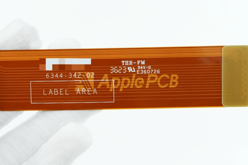
PCB marking is an important part of ensuring product compliance, traceability and quality control. It is also important in engineering reviews.
1.Special Marking Confirmation
When submitting a PCB order, please take care to check whether your design requires the following special markings:
- Environmental certification mark (e.g. Lead-Free, Pb Free)
- Safety certification mark (e.g. UL triangle mark ▲)
- XX mark (need to comply with IPC document requirements)
- Mark of origin such as “MADE IN CHINA”.
Please clearly indicate the type of marking required in your order and ensure that it complies with the corresponding standard specifications.
2.UL marking specification
Regarding the UL MARK labeling, special attention is required:
- Confirm whether the cycle format is correct (usually YYWW, WWYY format)
- Check whether the mark is located in the specified position of the sheet
- Please clearly mark the location information in the drawing.
- If there is a special shape of the cycle requirements, please specify in advance
Final Thoughts
The above contents are some of the parts of PCB engineering audit, but this is only the tip of the iceberg. PCB manufacturing is a complex engineering process, may also involve more specialized technical requirements, such as anti-soldering, drilling, plating, text, molding and many other process parameters. For more detailed information or technical support, please feel free to contact ApplePCB, our engineering team is ready to provide you with professional technical advice and support services.

