As a company specializing in PCB production for many years, we are well aware that our customers often encounter various technical problems in the design and production process. Based on our many years of production experience and technical accumulation, this article systematically organizes the PCB design and production process in the common six aspects of the problem and its solution.
Surface Treatment Process Issues
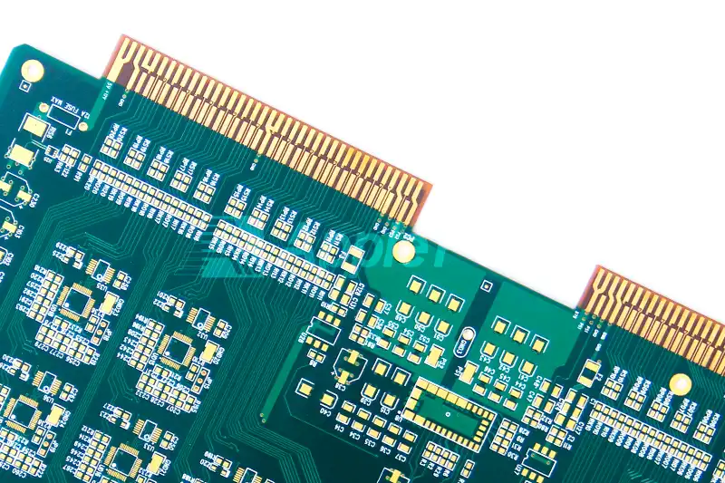
Why Do We Need to Do Gold Plating for Short and Long Gold Finger PCB's?
When designing PCBs that contain both short and long gold fingers, the traditional method of pulling gold leads will encounter difficulties in removing the leads when dealing with short gold fingers.
Solution:
Gold plating is recommended when the lead of short gold finger must be removed. The advantage of this solution is that the lead-free plating technique can be used to effectively avoid lead residue problems.
Why Is Copper Laid Down on the Inner Layer of Goldfinger PCBs?
As shown in the figure, we have compared the design of the inner layer of the gold finger without copper supplement (Fig. A) with the design of the inner layer with copper supplement (Fig. B). In practice, the design in Fig. B is obviously more reasonable. This is because, if the inner layer of the gold finger is not copper-assisted, it will lead to uneven flow of resin in this area. As the amount of flow varies, the curing of the resin directly affects the thickness consistency of the gold finger area, which in turn affects the overall tolerance control.
Why Is the Soldermask of the Sinking Tin Plate Easy to Come Off?
In the normal immersion tin process, we found that chemical fluxes are more aggressive to soldermask ink. When performing the 3M tape test, the ink on the pad edges tend to peel off, which may affect the reliability and life of the product.
Process Recommendation:
To ensure product quality, we recommend the following alternative processe to be considered:
- immersion gold process
- electroplating process
- silver Immersion Process
All of these process work well to protect the integrity of the soldermask.
Why Does Tin Spraying Process Lead to Uneven Surface?
In the PCB manufacturing process, tin spraying is a common surface treatment process. However, in the actual production, we often encounter the problem of uneven surface after spraying tin. Through years of production experience, this problem mainly stems from the following aspects.
First of all, in the process of PCB easy to warp deformation. This is mainly because in the tin furnace, the plate up and down uneven heat, resulting in inconsistent distribution of thermal stress. Especially when the plate thickness is thin, this phenomenon is more obvious.
Secondly, the characteristics of liquid tin will also affect the surface flatness. When the PCB into the tin furnace, the pad on the liquid tin will be subject to surface tension and the role of the arc. At the same time, the hot air blowing and gravity of the combined effect of the lower edge of the pad will form a solder sag phenomenon. This not only affects the appearance, but also creates problems for subsequent SMT placement - components may be shifted or tomb stoning may occur.
It is worth noting that there is a clear correlation between pad size and flatness: the smaller the pad, the more pronounced the effect of surface tension is, resulting in a more pronounced curvature of the solder surface and a consequent loss of flatness.
Solution:
Based on the above analysis, for the following cases, we recommend to carefully consider whether to use the tin spraying process: A. The pad size is small, the surface tension is more significant, resulting in more obvious curvature of the tin surface, the flatness decreases.
- BGA package boards with pad size less than 14mil.
- Products with strict requirements on surface flatness.
In these cases, it is recommended to choose alternative processes such as gold immersion or gold plating. Although the cost of these processes may be slightly higher, but can better ensure the surface flatness and the reliability of the subsequent process. Of course, if you specify the use of tin spraying, our engineering team will evaluate the process in advance to ensure that it meets your actual needs.
What Is the Difference Between Normal Immersion Tin and Nano Immersion Tin?
There are significant differences in tin layer thickness and performance between the two processes:
Ordinary immersion tin:
- Tin layer thickness: 1.0-1.5μm
- Risk of soldermask damage
- Longer cycle time
Nano-sinking tin:
- Thickness of tin layer: 0.35-0.55μm
- Significantly reduced risk of soldermask damage
- Processing time reduced.
- Cost savings of 10-20%
- Reduced rework and material waste
Substrate and Structure Issues
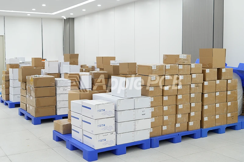
How Should PCBs Be Standardized for Storage?
Good storage environment requirements:
- Temperature: ≤ 25℃
- Relative humidity: ≤ 65%
- Environment: no corrosive gases, temperature control is required
General storage environment requirements:
- Temperature: ≤35℃
- Relative humidity: ≤75%.
- Environment: no corrosive gas
Use term recommendation:
- General PCB: recommended for use within 24 hours
- Chemical immersion tin/silver products: recommended to be used within 12 hours.
If PCB exceed the recommended shelf life, it can be dried and processed for trial use, and if necessary, the performance can be retested, and it can be continued to be used after passing the test.
What Causes PCB Warpage?
In the PCB manufacturing process, board warpage is a common but tricky problem. Excessive warpage not only affects the appearance of the product, but also bring serious trouble to the subsequent SMT soldering. Based on our production experience, the following factor are often the main causes of PCB warpage:
- Internal structure asymmetry
The symmetry of the internal structure of the PCB has a decisive influence on the flatness of the board. When the interlayer core board and semi-cured sheet arrangement is not symmetrical, in the thermal stress is very easy to produce warpage.
- Uneven distribution of copper area
When the difference between the copper foil area on the front and back sides of the PCB is too large, an imbalance of stress is generated within the material, which in turn leads to warpage. For example, a design with a large area of copper cladding on one side and only a small number of alignments on the other side is particularly susceptible to warpage after the etching process.
- Asymmetry of blind vias
In multilayer board design, asymmetric blind hole distribution can significantly affect the flatness of the board. For example, designing 1-3 layers of blind holes in a four-layer board without a corresponding balancing structure often results in warpage of the finished board.
Solution:
- Pay attention to the symmetry of the laminated structure at the design stage, and reasonably arrange the distribution of the core board and semi-cured sheet.
- For the outer layer wiring, try to keep the balance of copper foil area between front and back side. If a large area of copper cladding must be used on one side, it is recommended to add an appropriate grid-like area on the opposite side for balance.
When designing blind buried holes, a symmetrical structure should be used as much as possible. If a symmetrical design is indeed not possible, it is recommended to communicate with us in advance to negotiate the acceptable range of sheet warpage.
What Is the Difference Between “halogen-Free Sheets” and “halogen-Free Finished Products”?
- Halogen-free panels: only the base material is guaranteed to be halogen-free.
- Finished products are halogen-free: all raw materials must comply with halogen-free standards.
Therefore, you need to clarify the specific requirements when placing an order with the manufacturer.
What Specifications Should Be Followed When Designing Impedance Lines?
Major problems in impedance line design include:
- Inconsistent spacing of differential impedance lines
- Lack of required ground or power plane shielding
- Difficulty in distinguishing between characteristic impedance lines and differential impedance lines due to the same line width size.
To ensure accuracy of impedance control, it is recommended that:
- Differential impedance line design
- Maintain consistent line spacing
- Ensure a complete shield design
- Impedance line differentiation
When designing the PCB, traces both are single used ended and and thus differential it impedance is advisable to distinguish between the two by varying their line widths slightly.
For instance:
Single-ended impedance line: 4mil
Differential impedance line: 4.1mil
Depaneling Process Issues
In the PCB production process, the depaneling process often encounter some technical difficulties. Below we analyze several typical problems in detail.
Bridge Width Problem?
Problem: The width of the bridge is too large, which makes it difficult to separate the boards after patching.
Solution: Optimize the width of the bridge by adding stamp holes at the appropriate locations.
What if the PCB Is Too Thin for V-CUT?
Problem: The thickness of the board is lower than the minimum requirements of the process (0.6mm), can not realize the V-CUT process
Solution:
- Recommended to change the stamp hole connection method
- Change to single-sided V-CUT.
V-CUT Spacing Issues?
Problem description: The spacing between the plate is less than the process requirement (minimum 2mm), and the standard V-CUT process cannot be realized.
Solution:
①adjust the pitch to 2mm and adopt double-blade V-CUT process.
②change to zero-pitch program
③adopt single-knife V-CUT in the middle of the collage.
Drilling and Plating Process Issues:

What Are the Differences Between Different Over-Hole Processes?
In PCB manufacturing, there are four main categories of over-hole treatments, each with its own specific application scenarios:
1.Over-hole covering
Characteristics: The surface of the pad is covered with solder resist ink.
Limitations: the hole wall is not guaranteed to have ink coverage
Application: generally used for the need to protect but not strict requirements for the hole wall occasions
2.Vias with windows
Characteristics: No soldermask on the pad surface or hole wall.
Application: Suitable for applications that require subsequent filling or special treatment.
3.Hole Plugging
Characteristics: The pads are covered and the holes are completely filled with soldermask.
Advantage: Provides the most complete protection
Application: For applications where the walls of the holes need to be protected from solder sticking.
In order to avoid subsequent communication barriers and quality disputes, we strongly recommend:
- Specify the specific requirement of the perforation process when placing an order.
- Fully understand the characteristics and limitations of the various perforation processes.
Our team of engineers is always ready to provide you with technical advice and help you choose the most suitable process solution.
What Are the Process Requirements for Plating and Filling Holes in the Disk?
Depending on the size of the hole, different filling times are used:
- ≤0.25mm: single hole filling
- 0.3-0.45mm: double hole filling
- 0.5mm: Hole-in-dish process is not recommended.
Recommendation:
1.Prioritize small hole design (≤0.25mm)
2.The thickness of copper plating can be more than 50μm, which is enough to meet the electrical performance requirements.
3.Considering the production efficiency, it is recommended to avoid the use of large aperture design.
SMT Process Issues:
SMT Pad Design Should Pay Attention to What?
- Large pad size: wave soldering of large component pad need to be appropriately increased, SOT23 pad is recommended to lengthen 0.8-1mm. the purpose is to prevent the “shadow effect” resulting in empty welding
- Pad size matching: disk width should be equal to the component electrode width or slightly larger to ensure the best welding results, to avoid false welding or bias.
- Try not use large pads: In this case, avoid placing a large pad in between two components. The pads should be placed separately and connected with thin wires in between. When connecting wires it can be done in parallel in the event that there is need of large current.
- Do not place through holes near the pads: It is also important that through holes are not designed on or around the pads in order to avoid loss of solder during reflow soldering hence leading to false soldering or lack of solder or even short circuit.
How Should SMT Components Be Reasonably Laid Out?
1.The long axis of the components is perpendicular to the direction of the conveyor belt: preventing component drift and the phenomenon of “vertical monument”.
2.Uniform distribution of high-power devices: to avoid local overheating and ensure the reliability of the solder joints.
3.Double-sided mounting of large components need to be staggered layout: to prevent excessive local heat capacity, to ensure the quality of welding.
4.The long axis of large SMT devices is parallel to the direction of solder wave flow: reduce the solder bridge between electrodes.
5.Large and small devices need to be staggered layout, avoid straight line arrangement: to prevent the “shadow effect” caused by false soldering and leakage of solder.
6.Avoid placing PLCC/QFP and other four-sided pin devices on the wave soldering surface.
Wrapping Up
With this article, we summarize the experience we have gained over many years of communication with our customers and in actual production. These problems and solutions are derived from many real cases of cooperation. We hope that this sharing can help you avoid potential problems, improve product yields and shorten development cycles. If you have any questions, please feel free to contact us! As a partner specializing in PCB manufacturing for 15 years, we are willing to explore better solutions with you!

