In our digitally interconnected world, seamless communication between devices is paramount. Every action, command, or data transfer relies on precise interactions between multiple circuit boards. By ensuring immediate connections, gold fingers play a crucial role in this process, acting as the bridge that quickly relays signals from one circuit board to the main processing unit.
What is Goldfingers PCB?
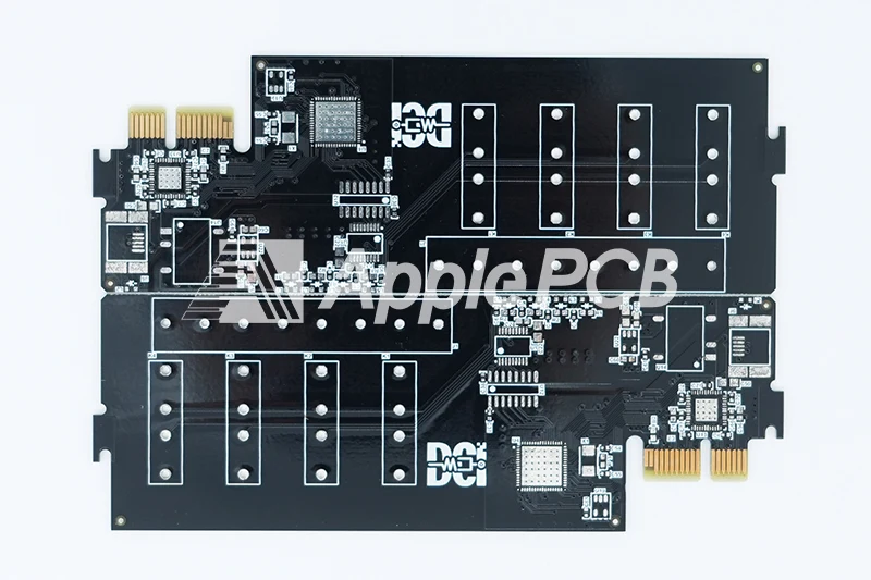
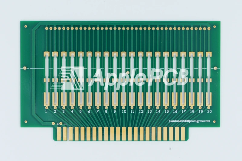
A goldfinger PCB is a type of printed circuit board characterized by gold-plated connectors located on one or more edges. The distinctive layout of these gold-plated pads resembling fingers, earned them the name "gold fingers". This design is crucial for establishing reliable, high-durability connections in electronic devices where frequent plugging and unplugging are required.
Types of Goldfinger PCB
Common goldfinger PCB (flat gold finger): Uniform distribution with pads of the same length and width.
Different length goldfinger (crooked gold finger): Pads have the same width but varying lengths and spacing.
Segmented PCB (discontinuous gold finger): Pads vary, and gold fingers are cut into multiple sections.
Advantages and Applications of Goldfinger PCB
Advantages
● Superior Conductivity
Gold boasts exceptional electrical conductivity, minimizing signal loss and ensuring efficient data and power transmission. This is crucial for goldfingers, as they establish critical connections between the PCB and other components. Unimpeded signal flow translates to reliable performance and data integrity within the electronic device.
● Corrosion Resistance
Gold and copper display contrasting behaviors when it comes to corrosion. Copper is susceptible to corrosion, from chemicals, moisture or electrolytic conditions whereas gold serves as a barrier and exhibits exceptional resistance.
● Exceptional Wear Resistance
Goldfingers inherent durability and resistance to wear make them ideal for withstanding insertions and removals from connector slots.
Applications
● Memory Modules (RAM, ROM, SSDs)
These components depend on gold connectors to create high speed links, with the motherboard enabling data exchange.
● Expansion Cards (Graphics Cards, NICs)
Expanding a computers functionalities involves adding expansion cards that connect to the motherboard via gold connectors. This allows for increased processing capabilities or network connections.
● Mobile Devices
The strong connections, in your smartphone or tablet are thanks to gold contacts. These connections help connect parts, like batteries, screens and cameras to the circuit board ensuring smooth performance.
● Automotive Electronics
Gold Finger PCBs are prevalent in dashboard's digital displays, car audio, entertainment unit, GPS.
● Home Entertainment Systems
Gold finger PCB play a crucial role in high definition TV, gaming consoles and audio equipment.
● Office and Industrial Equipment
Goldfinger PCBs are essential in printers and scanners, automation and control systems, equipment used for testing and measuring.
Manufacturing of Goldfinger PCB
Manufacturing goldfinger PCB involves additional procedures compared to regular PCBs because of the gold fingers, these gold fingers need plating and inspection for dependability.
Gold Plating
To prolong the lifespan of gold plated connectors they are often coated with a layer of gold, through a series of steps including cleaning, pre-plating, electroplating and post-plating processes.
Edge Beveling
The beveled edges of gold finger PCBs can facilitate insertion and extraction of the PCB from the connector.
Quality Control
Since gold fingers are the handshake between the PCB and the connector, they gotta be top-notch. That's why gold finger PCBs get a super close inspection. This includes visual inspection, electrical testing, and dimensional checks.
Surface Finish for Golden Finger PCB
Hard Gold Plating / Electroplating Nickel Gold
Hard gold plating involves a percentage around 3%- 5% of additional metals like cobalt or nickel into the gold layer. This alloying technique significantly boosts the toughness and longevity of the gold while also preserving its notch conductivity. This is essential for goldfingers that undergo repeated insertion and removal cycles, guaranteeing reliable connections throughout a prolonged usage period.
Advantages
Exceptional Wear Resistance: Due to the incorporation of other metals like cobalt or nickel, hard gold offers the highest wear resistance among these three options. This makes it ideal for applications with frequent mating cycles e.g., mobile phones, connectors.
The cost of hard gold plating may be lower than that of ENIG, especially for large area or high volume production.
Disadvantages
Soldering Challenges: The presence of other metals in gold can pose challenges when soldering compared to ENIG or ENEPIG.
ENIG (Electroless Nickel Immersion Gold Plating)
ENIG is the most common type of gold plating for goldfingers. ENIG involves a chemical process than electroplating. ENIG comprises two layers: nickel and gold. Firstly a nickel layer is applied to the copper pads, then gold layer is deposited through a replacement reaction on the nickel. Note that the surface gold layer is pure gold, not an alloy. The nickel layer protects the copper, from oxidation and corrosion while the gold layer shields the nickel underneath.
Advantages
Great Solderability: The nickel coating in ENIG is perfect for soldering components onto the PCB.
Cost Effective: Contrasted to hard gold, ENIG is a more economical choice.
Disadvantages
In the earlier days when manufacturing techniques were less advanced, ENIG often led to a phenomenon known as "black pad" during the soldering process.
Lower Wear Resistance: Since the top layer of ENIG treatment is pure gold, it is much softer than hard gold plating, leading to less contact force at only 35 grams or less and fewer usage cycles.
Thinner Gold Layer: The immersion gold layer in ENIG is very thin, which in rare cases of high-frequency applications, could introduce some signal loss.
ENEPIG (Electroless Nickel Immersion Gold)
The ENEPIG consists of three layers, nickel, palladium and gold. To start a nickel layer is applied to the copper pads using a nickel electroless solution. Next a palladium layer is added on top of the nickel through a replacement reaction. Finally a gold layer is plated onto the palladium layer using a salt solution, in another replacement reaction.
Advantages
By incorporating nickel, palladium and a gold, ENEPIG offers superior wear resistance in comparison to ENIG. This specific plating is ideal for demanding situations that require mating cycles.
Disadvantages
The most expensive surface finish, as the use of precious metals such as palladium.
Check Our Manufacturing Capabilities
| Feature | Capability |
| Materials | FR4, Rogers, Shengyi, Tuc, etc. |
| Max Layers | 1-40L |
| Min. Hole Size | 8mil/0.2mm |
| PCB thickness/hole size ratio | Maximum:12:1 |
| Gold Thickness | Hard Gold: 2 to 50µ" |
| ENIG: 1 to 5µ" | |
| Board Thickness | 0.2-8mm |
| Min. Trace Width | 0.08mm |
| Min. Trace Space | 0.08mm |
| Minimum space finger to beveling for avoid damage fingers | 0.15mm |
| Surface Finishing for Goldfinger | Hard Gold (Electrolytic Gold), Immersion gold(ENIG), ENEPIG, ENIG+OSP, HASL+plating hard Gold, ENIG+plating hard Gold, OSP+plating hard Gold, etc. |
| Solder Mask | Green, Red, Yellow, Blue, White, Black, Purple, Matte Black, Matte green |
| Silkscreen | White, Black, Red, Purple, etc. |
| Via Process | Tenting Vias, Plugged Vias, Vias not covered |
| Test | Fly Probe Testing (Free) and A.O.I. testing |
| Build time | 5-10 days |
| Lead time | 2-3 days |
| Certifications | ISO 9001:2015 |
| UL | |
| ROHS | |
| REACH | |
| Quality Standards | IPC A-600,IPC-6010 |
Design for Manufacturability of Gold Finger Boards

Chamfering of Gold Fingers
Connector pins that are gold plated feature slanted edges to make it easier to insert them and decrease wear and tear from frequent use. The angles of the chamfers typically range from 20°, 30° to 45° depending on the design needs and type of connector.
Solder Mask Clearance
Make sure to handle the solder mask, around the gold fingers with care. It's important to ensure that the solder mask doesn't cover the gold fingers to avoid any disruptions to the connections. This separation guarantees an straight connection, between the gold fingers and the mating connector.
Spacing Between Pads and Gold Fingers
It is crucial to ensure there is at a 1.0 mm gap, between the circuit board fingers and adjacent solder pads or components on the PCB to avoid electrical shorts or solder bridging.
Orientation of Gold Fingers
When beveling the PCB edges, avoid gold fingers facing inward so they do not point towards the center of the PCB. This minimizes the risk of damage and facilitates easier access during assembly.
Avoid Proximity to PTHs
Make sure to keep circuit board gold fingers from plated through holes (PTHs) to avoid any disruptions, during the plating and assembly stages.
Design Considerations for Gold Finger Beveling
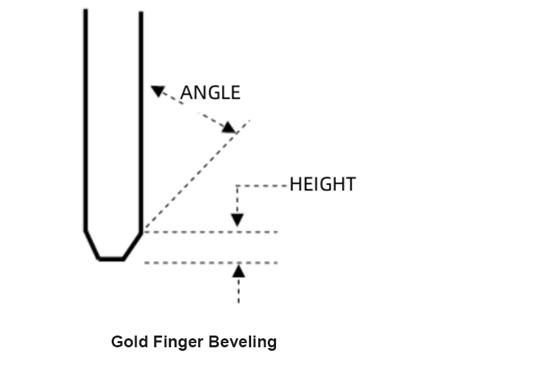
Bevel Height
The distance measured vertically from the edge of gold finger to the starting point of the bevel (or chamfer), and we call it the bevel height.
Bevel Angle
The bevel angle, typically set at 45 degrees, is the angle at which the edge of the gold finger is cut or shaped.
Bevel Tolerance
Bevel tolerance is the allowable deviation from the specified bevel dimensions (height and angle).
PCB Size on Bevel Design
The combined size of the panel should respect the minimum dimension of 50mm x 50mm.
Thickness Requirements
The recommended minimum thickness for a PCB undergoing gold finger beveling is ≥0.6mm. Thinner PCBs may not support a robust bevel.
Copper Clearance
Copper clearance, also referred to as copper reduction or copper backoff is a method employed to eliminate or withdraw copper from the PCBs edge in beveling. It is essential that the copper layers remain unexposed throughout the beveling process. The standard rule for copper clearance is the bevel height plus an extra 0.4mm.
Outward vs. Inward Facing Bevels
Outward facing gold fingers are located at the outer edge of the panel, allowing the bevels can be beveled in one go using beveling machine, which makes the process faster and cost-effective.
Inward facing gold fingers are not located at the outer edge of the panel but rather positioned inside the PCB, often because other parts of the PCB extend beyond them. This necessitates the utilization of computer controlled beveling equipment, where a tailored program is created to instruct the machine on cutting each gold fingers' bevel at an angle and height resulting in enhanced accuracy, at an increased expense. (Note that bevel can not be processed with the inward facing gold fingers.)
What Determines the Quantity of Gold Fingers?
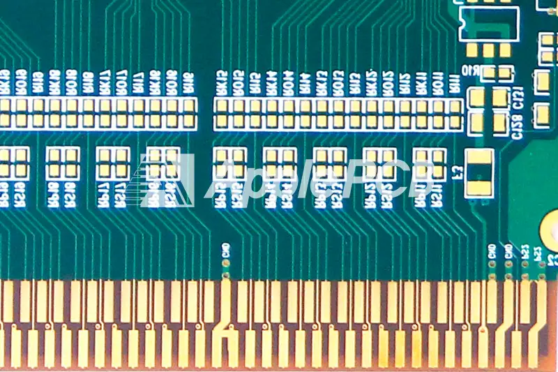
Factors Determining Gold Finger Quantity
The number of gold fingers on a PCB varies depending on the design and application requirements.
The size and shape of the PCB kind of dictate how many gold fingers it needs. Think of it like real estate - bigger boards have more space for more fingers, while oddly shaped ones might have some tight corners where fingers wouldn't fit.
The number of signal and power lines on the PCB affects how many gold fingers it needs. Basically each signal or power line usually gets its own gold finger to keep everything running smoothly.
Various connectors come with Various numbers of pins. Its crucial for the gold contacts to align perfectly with these pin quantities.
Impact of Gold Finger Quantity
The number of gold fingers on a PCB impacts its functionality in several key ways. Too few fingers can lead to unreliable connections, signal issues, and even power delivery problems. For optimal performance, the right amount is crucial for maintaining good signal integrity, handling high currents, and even aiding in heat dissipation. They also contribute to EMI/RFI shielding, with more fingers offering better protection.
Consult with ApplePCB for Quote
ApplePCB provides quotes based on the gold fingers' area of the PCB. Including the dimensions and the number of gold fingers in your specifications helps us accurately calculate the area and provide a precise quote.
Why Choose ApplePCB?

Premium Gold Plating Service
As a finger PCB manufacturer, ApplePCB offers premium gold plating for all your PCB needs. Our ENIG plating delivers gold thickness up to 4µ", ideal for applications requiring excellent corrosion resistance and solderability. For superior wear resistance, our hard gold plating reaches up to 50µ", perfect for high-contact uses. Kindly inform us the thickness of the gold plating needed (options from 2µ" to 50µ") and the number of gold fingers for your PCB. With these details, we can furnish you with a competitive quotation within 1 hour.
A Variety of Goldfinger Designs
ApplePCB specializes in various gold finger designs, including standard, segmented, and custom length options across in single-layer, double-layer, and multi-layer, with ENIG, ENEPIG or hard gold plating to achieve the best performance for your project.
Exceptional Quality
To ensure top performance and durability, ApplePCB upholds our dedication to quality through our ISO9001:2015 and UL certifications, every PCB undergoes quality checks, including 100% electronic testing and thorough AOI (Automated Optical Inspection).
FAQ about Goldfinger PCB
How to save goldfinger PCB’s cost?
To reduce costs, ApplePCB offers a combined solution: HAL (Hot Air Leveling) for the non-critical areas of the PCB surface and gold plating specifically for the gold fingers. This method, known as HAL + Gold Finger Plating, is ideal when the trace width, pad gap, and soldering requirements are moderate.
Is gold in gold fingers real gold?
Let’s look at two concepts associated with the gold finger: soft gold (pure gold) and hard gold (alloy). Hard gold typically involves alloying gold with other metals like nickel or cobalt. These alloys make the gold layer much harder and more durable than pure gold. In contrast, soft gold is nearly pure gold, typically around 98% purity. No matter plating soft gold or hard gold, the gold content is minimal.
How much gold is in gold fingers?
When it comes to ENIG (Electroless Nickel Immersion Gold) finishes, the gold layer typically around 2 to 5µ". On the hand, electroplated gold can easily reach thicknesses of 15µ" or more.
Why is there a nickel layer between gold and copper?
When gold and copper come into direct contact, their distinct electrochemical characteristics lead to electromigration, where copper atoms move into the gold layer creating a copper gold alloy at the interface, this alloy can weaken the electrical performance of the gold layer. To address this issue a nickel layer is electroplated between the copper and gold layers to act as a barrier layer.
What is flash gold of the surface finish in PCB production?
Before applying a hard gold electroplating on a PCB, a process known as flash gold plating is employed. This method entails utilizing currents and a concentrated gold solution to form a thin gold coating on the nickel surface.
Flash gold significantly reduces costs and time. Because it skips the full steps of gold electroplating. Nevertheless the thinner gold layer can affect the durability of PCB.
