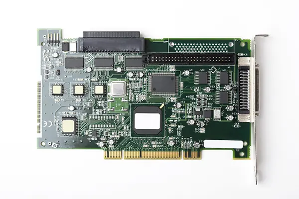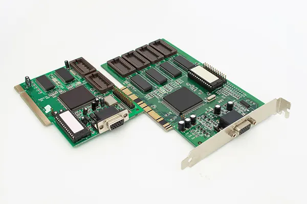
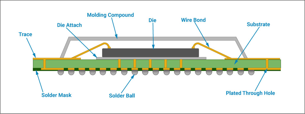
When working with Ball Grid Array (BGA) packages, a specific assembly process is required to connect them to Printed Circuit Boards (PCBs). This process involves soldering the BGA package onto the board using its numerous surface-mounted solder balls. These tiny spheres act as the bridge between the BGA's internal connections and the PCB's circuitry.
To achieve this connection, the BGA is carefully positioned on the board and then subjected to controlled heating. This melts the solder balls, forming strong electrical connections between the BGA and the PCB. The precision and reliability of this soldering method make it ideal for applications demanding a high degree of accuracy.
Furthermore, BGAs offer a significant advantage in situations where space is limited. Their compact footprint allows for greater miniaturization compared to other packaging options. This makes them particularly valuable for modern electronic devices that prioritize both functionality and small size.
When your electronics project demands high-performance components in a compact footprint, BGA assembly offers a compelling solution. This popular surface-mount packaging technology delivers both high density and cost-effectiveness, making it ideal for a wide range of electronic components.
At ApplePCB, we boast extensive expertise in BGA assembly services, earning the trust of clients with even the most intricate designs. Regardless of your project's size or complexity, we possess the capabilities and experience to fulfill your unique requirements. We prioritize accuracy in every BGA PCB assembly and rework project, employing rigorous testing methodologies to guarantee reliability. Our services cater to a diverse array of industries, including consumer electronics, miniature electronics, automotive, LED, medical, wireless and telecommunications, satellite, and many more.
Types of BGA PCB
When working with printed circuit boards, you'll encounter various BGA configurations. Each type offers unique advantages and suits specific applications.
1. Flip Chip BGA (FCBGA)
This BGA type eliminates the need for pins or leads by directly soldering the chip to the circuit board. This approach results in a compact footprint and improved electrical performance.
2. Ball Grid Array (BGA)
This popular BGA configuration features a grid of solder balls arranged in an array. These balls create reliable connections between the component and the PCB.
3. Land Grid Array (LGA)
Similar to BGA, LGA utilizes an array of copper pads instead of solder balls for connections. This design offers high density and excellent thermal performance.
4. Ceramic Ball Grid Array (CBGA)
CBGA packages employ a ceramic substrate with an array of solder balls. This construction provides robust electrical connections and excels in applications demanding high temperature, shock, and vibration resistance.
5. Tape BGA
This unique BGA type utilizes tapes instead of solder balls for component connections. This method proves advantageous in designs where space and cost are critical factors.
6. Plastic Ball Grid Array (PBGA)
PBGA packages utilize plastic as the base material, offering reliable electrical performance and resilience against temperature fluctuations, shock, and vibration.
Steps of BGA Assembly
The process of assembling BGAs onto PCBs involves a series of precise steps to ensure proper functionality and long-term reliability. Let's walk through each stage of this intricate process:
1. Preparing the PCB
The journey begins with the PCB. Solder paste, a crucial mixture of solder alloy particles and flux, is carefully applied to the designated pads where the BGA will reside. This paste acts as the glue that will bond the BGA to the PCB during the soldering process.
2. Placing the BGAs
Next, the BGAs, essentially integrated circuit chips adorned with solder balls on their underside, are meticulously positioned onto the prepared PCB. This task is typically entrusted to automated pick-and-place machines, ensuring accuracy and efficiency.
3. Reflow Soldering
With the BGAs in place, the PCB embarks on a journey through a reflow oven. Inside, the PCB is subjected to a specific temperature profile, causing the solder paste to melt and the BGA's solder balls to reflow. This molten dance culminates in the formation of robust electrical connections between the BGA and the PCB pads.
4. Cooling and Inspection
Following the fiery reflow process, the PCB is gently cooled, allowing the solder joints to solidify. A meticulous inspection then ensues, utilizing techniques like automated optical inspection (AOI) or X-ray inspection to identify any potential defects such as misalignment, shorts, or open connections.
5. Secondary Processes
Depending on the specific needs of the product, additional steps may be taken to further enhance its reliability and quality. These can include cleaning, testing, and applying a protective conformal coating.
Advantages of BGA Assembly
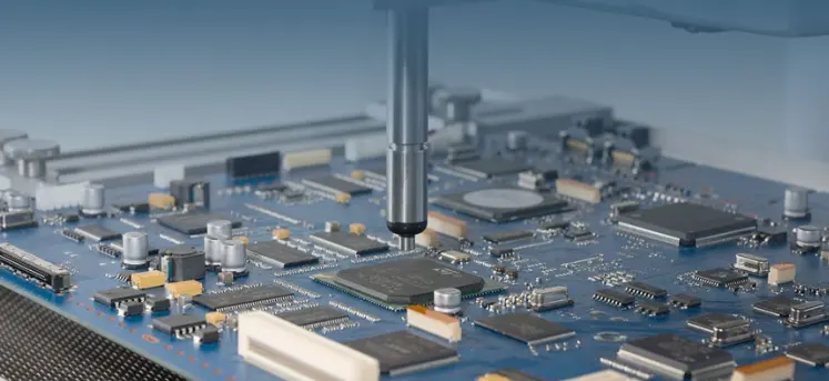
As technology advances, electronic devices are getting smaller yet more intricate, with BGAs becoming a crucial component in modern circuit design. These ball grid assemblies provide various advantages compared to conventional packaging methods, making them a popular choice among engineers and manufacturers.
Miniaturization in Electronics
One of the most significant advantages of BGAs is their ability to facilitate miniaturization. With the ever-growing demand for smaller and more portable electronics, BGAs offer a space-saving solution by utilizing solder balls for connections instead of traditional pins. This allows for significantly more connections within a smaller footprint, contributing to the development of compact yet powerful devices.
Improved Performance at High Speed
Beyond miniaturization, BGAs also boast improved performance at high speeds. The robust interconnections created by the solder balls ensure a reliable connection even under demanding conditions. This, coupled with the reduced warping facilitated by the BGA structure, allows for superior electrical performance at high frequencies.
Reduced Component Damage
BGAs offer a distinct advantage in terms of component damage mitigation. The unique soldering process employed by BGAs, where the solder balls are melted to form connections, significantly reduces the risk of damage to sensitive components during assembly. This is particularly crucial for intricate and delicate circuits.
No Pin Bridging
In traditional pin-based packages, the close proximity of pins can lead to solder bridges forming between them, causing electrical shorts and malfunctions. BGAs, with their strategically placed solder balls, effectively eliminate this risk, ensuring reliable and consistent connections.
Efficient Use of Space
Unlike conventional packages that require space for pin connections around the periphery, BGAs allow for connections to be made both around the edges and underneath the package itself. This opens up valuable real estate on the PCB for other components, optimizing the overall layout and design.
Low-inductance Leads
The short distance between the PCB and the package minimizes inductance, resulting in cleaner and more efficient signal transmission. This is particularly important in high-speed applications where signal integrity is paramount.
BGA Assembly Service Features
ApplePCB is capable of delivering both high-quality and economical BGA assembly services for your printed circuit boards. We have the capability to handle BGA assembly with a minimum pitch ranging from 0.2mm to 0.3mm. We offer PCB assembly services containing the following BGA types:
- Plastic BGA (PBGA)
- Ceramic BGA (CBGA)
- Micro BGA
- Micro Fine Line BGA (MBGA)
- Stack BGAs
- Leaded and Lead-free BGAs
We also provide assembly services for ultra-fine pitch Quad Flat Packages (QFP), Quad Flat No-Lead Packages (QFN), and Chip Scale Packages (CSP).
To ensure the highest quality assembly, our team meticulously analyzes BGA datasheets, taking into account size and ball material composition. We then optimize the thermal profile of the BGAs, further enhancing the integrity and performance of your PCB assembly.
Ensuring BGA Assembly Quality with X-ray Inspection
At ApplePCB, we understand the critical role of BGA components in modern electronics. To guarantee their proper assembly and functionality, we utilize advanced X-ray inspection technology. This allows us to identify potential soldering issues, such as solder balls and paste bridging, with unparalleled accuracy.
Our X-ray inspection program goes beyond simple detection. It can also calculate the precise gap size of each solder ball, ensuring compliance with your specified IPC Class II or Class III standards. Additionally, our skilled technicians can utilize 2D X-ray images to reconstruct detailed 3D representations of the BGA assembly. This enables them to thoroughly inspect for hidden problems, including damaged PCB vias and cold solder joints.
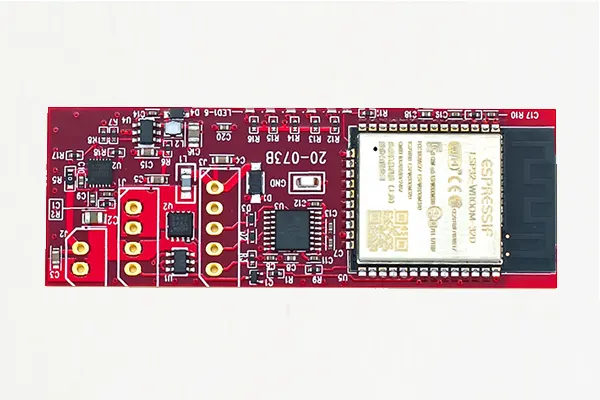
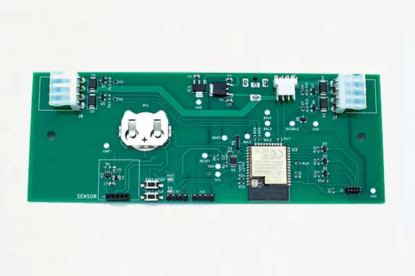
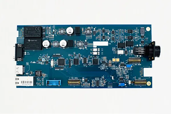
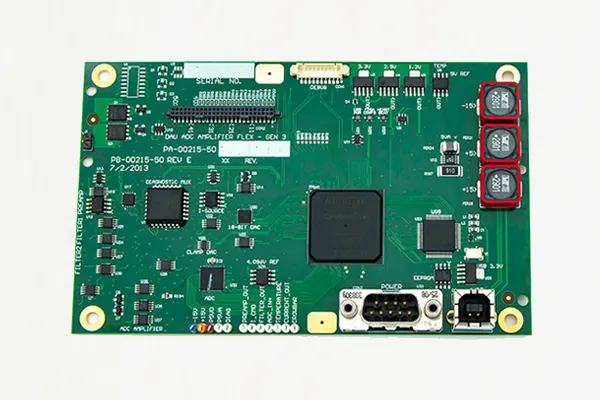
Our BGA Assembly Examples
With over a decade of experience in PCB assembly, ApplePCB possesses the expertise and resources to fulfill your BGA assembly needs. If you require BGA assembly services, please don't hesitate to contact us. We are confident in our ability to deliver high-quality results that meet your exact specifications.

