The demand, for more lightweight and compact electronics is rising, leading to an increased need for HDI PCB in the electronics industry.
A recent report predicts that the global market for high density interconnect PCBs (HDI) will experience a 5.5% growth rate from 2023, to 2028 reaching a market value of $11.5 billion by 2028.
Therefore, choosing a quality HDI PCB manufacturer will help your organization to stand out in the competitive market and gain greater market share and customer trust. In this article we will introduce you to HDI PCB application scenarios, structures, types, material selection as well as design and manufacturing difficulties.
What is a HDI PCB?
HDI PCBs are known as HDI leiterplatten, HDI PCB prototype, and high-density interconnect PCBs which have a higher wiring density compared to other PCBs. In a scenario where a standard multilayer PCB requires ten layers to create a circuit an HDI PCB can achieve the functionality, with 8 or fewer layers. This efficiency is due to the use of smaller vias, pads, copper wires and denser wiring, in HDI PCBs. With these design an HDI PCB can potentially consolidate the functionality of PCBs into one ultimately saving valuable space within the device. The main application areas of HDI PCBs:
Smartphone and Tablet PC
Smartphones and tablet PCs benefit from HDI boards due, to their ability to accommodate circuits and fit more components in a confined space making them ideal for devices with limited space yet demanding high performance.
Wearable Devices
Wearable devices can be made lighter and smaller with the help of HDI boards as they enhance wiring density and reduce layer count also meeting the requirements, for performance and extended battery life.
Automotive Electronics
HDI boards maintain reliability in high-temperature and high-vibration environments thanks to their compact construction and excellent electrical performance. They also play a key role in control modules for advanced driver assistance systems (ADAS), infotainment systems, and electric vehicles.
Medical Devices
The HDI board's high-density wiring capability and excellent electrical performance ensure precision and reliability, while its compact structure meets the needs of some implantable devices and small probe instruments. Therefore, it plays a key role in medical imaging, portable diagnostics and life monitoring equipment.
Military Aerospace
HDI boards offer excellent reliability, signal integrity and high-speed data transmission capabilities, making them the choice for military communications equipment, aerospace equipment.
Different Types of HDI Circuit Boards
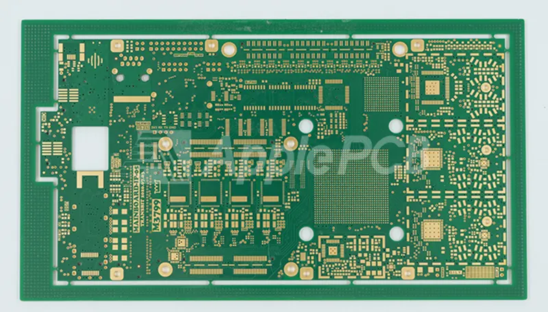
In response to market demand, ApplePCB has the capability to combine flexible PCB technology with HDI PCB technology to provide customer with flexible, rigid-flex HDI PCB.
Typical HDI PCB
Typical HDI PCB use a rigid substrate such as FR4 material. These HDI PCB utilize microvia and fine pitch technology to achieve high density wiring for application requiring durability and stability.
● Flexible HDI PCB
In contrast to typical flexible PCBs, Flexible HDI PCBs often utilize kapton as a material to meet high frequency, high speed and flexibility requirements. By combining a very small bend radius with HDI technology, Flexible HDI PCBs can better optimize the internal space layout. Often found in wearables and mobile devices.
● Rigid-Flex HDI PCB
Rigid-flex PCB combine flexibility and stability, saving the use of connector. HDI PCB has the advantage of high-density cabling. The Rigid-Flex HDI PCB combines the advantages of both. It helps our customers to build more integrated and reliable devices, typically in high-end consumer electronics and aerospace equipment.
How to Choose Materials for HDI PCB?
When choosing materials for PCB HDI that need to handle high-speed signals the key factors to consider include the operating frequency of the dielectric (measured in Gbps/GHz) and the acceptable level of signal loss (dB).
1. Normal Speed and Normal Loss
These are common standard materials such as the FR4 series. These materials have relatively moderate dielectric constants and loss factors and are typically used for low frequency applications up to 5 GHz. Isola FR370HR is a typical representative of these materials, in addition to which we can also provide you with materials such as EM-827(I), EM-370(Z), Nelco N7000-2HT and others.
2. Medium Speed and Medium Loss
These materials are able to maintain more stable values of dielectric constant over frequency changes and have lower dielectric loss (roughly half that of normal speed materials). They are therefore suitable for use in applications with operating frequencies of 0-10 Hz and dissipation factors of 0.012-0.007. Common materials are FR408HR and Isola I-Speed.
3. High Speed and Low Loss
In applications that require high speed transmission and low loss, such as automotive electronics and advanced communications equipment, materials with low dielectric constants and low loss factors need to be selected. These materials excel in the 10 to 30 GHz frequency range, with loss factors typically ranging from 0.0095 to 0.0022, while they maintain lower electrical noise. ApplePCB can provide you with EM-528, I-Tera MT40, and Megtron R-5775.
4. Very High Speed and Very Low Loss (RF/Microwave)
If your HDI circuit board needs to be used in RF/microwave applications, then you need to choose materials with ultra-high speed and very low loss. These material can perform well in 20-60 GHz applications and they have extremely low dielectric loss (Df ≤ 0.0021). ApplePCB can offer you a choice of materials as diverse as Isola Tachyon 100G, Rogers 4350B and Megtron6 R-5775, for this category.
The Structure of HDI PCB
Depending on the design requirement, HDI printed circuit board can utilize different layering method to achieve the desired. Below are a few common type of HDI PCB structures:
1. Simple HDI Structure (1+N+1)

This structure contains a high-density interconnect layer for BGAs with low I/O counts. it features fine wires, microvias, and positioning techniques that enable 0.4 mm ball spacing, provide excellent mounting stability and reliability, and may contain through-holes filled with copper. Typical applications include cell phones, MP3 players, GPS and memory cards.
2. More Complex HDI Structures (2+N+2)

HDI PCB boards in this configuration contain 2 or more high-density interconnect layers. The microvias on the different layers can be interleaved or stacked; copper-filled stacked microvia structures are common in challenging designs requiring high levels of signaling performance. Stacked microvias can be more expensive due to their higher precision requirements. These structures are suitable for BGAs with smaller ball pitches and higher I/O counts. And is commonly used in mobile phones, PDAs, game consoles, and portable video equipment.
3. Every Layer Interconnect (ELIC) Structure

In this HDI multilayer PCB structure, all layers are high-density interconnect layers, allowing conductors on any layer of the board to be freely connected to the copper-filled stacked microvia structure. This structure provides a reliable interconnect solution for highly complex, large pin-count devices such as CPU and GPU chips used in handheld and mobile devices, while yielding superior electrical characteristics. Applications include cell phones, ultra-portable PCs, MP3, GPS, memory cards and small computer devices.
However, the more laser drilled holes, the more demanding the HDI PCB manufacturing technology becomes. In today's market, electronic end products are primarily 3rd, 4th, and 10 or 12 layer Anylayers. very few manufacturers are able to build higher order HDI or higher layer count Anylayers, but ApplePCB is able to build HDI PCBs up to 40 layers and up to 7th order, and you can view our HDI PCB fabrication capabilities in the table below.
ApplePCB's Manufacturing Capabilities
| Item | Performance Parameter |
| Layer Count: | 4-40L |
| Stack-up | From 1+N+1 to 7+N+7 |
| PCB Via | Blind via, Buried via, Staggered via, Stacked via, Skip via |
| Space Between Through Hole and Blind Via. | Minimum 8mil |
| Minimum Laser Drill Diameter | 0.01MM |
| Minimum Trace Width/Space | 2mil/2mil |
| Min BGA pad. | 8mil |
| High Frequency Mixed HDI | Ceramic,PTFE just can do machine drilling for blind or buried via, or back drilling,(can't do laser drilling) |
| PCB Thickness: | 0.4-8mm |
| Thickness Tolerance: | ≤1.0mm: +/-0.10mm, |
| >1.0mm:+/-10%. | |
| Minimum PCB Size | 2.5x2.5mm need create panel, 10x10mm can do single board. |
| Minimum PCB Size | 500x600mm |
| Outline Dimension Tolerance: | Standard;±0.13mm, |
| Minimum:±0.10mm. | |
| Maximum Copper. | 3oz |
| Impedance Control | 90Ω ~100Ω |
| Technical Feature | 90Ω & 100Ω Differential impedance, thick cooper |
| Surface Finish Technology | Plating NI/AU, plating hard Gold, ENIG, Immersion Tin, Immersion silver, OSP, ENIG+OSP, ENIG+plating hard Gold, plating gold+plating hard Gold, ENEPIG, OSP+plating hard Gold. |
Problems That May Occur in HDI PCB Design
1. Crosstalk
Since the signal alignment of HDI PCBs is very tight, signals from adjacent traces tend to interfere with each other, resulting in signal distortion, data corruption and other problems.
When this occurs, ApplePCB recommends that you increase the spacing between signal traces, minimize parallel runs and crossovers or use ground and power layers as shields.
2. Impedance Discontinuities
In HDI PCBs, impedance discontinuity is a change in the characteristic impedance of the signal traces, resulting in signal reflection and performance degradation, which is usually caused by vias, changes in the width of the traces, or bending of the signal traces.
To solve this problem, we should try to maintain consistent alignment widths and spacing throughout the signal path, use impedance-controlled vias and vias transitions, implement back-drilling and buried vias techniques to reduce the vias' short cutoff line effect, and carefully design alignment bends and corners to minimize impedance mismatch. These measures effectively reduce the impact of impedance discontinuities on signal transmission, thereby improving the overall performance and reliability of HDI boards.
3. Power Integrity Issues
Power integrity is especially critical in HDI PCB, where high component density and high-speed signal can cause power problems such as voltage drop, simultaneous switching noise (SSN) and ground bounce.
To ensure power stability, consider placing decoupling capacitor near power pins, using solid-state power and ground layers for efficient power distribution, and isolating noisy circuits with proper power plane segmentation. In addition, the power and grounding layers need to be carefully designed to minimize impedance and inductance. These measures help minimize power problems and ensure the performance and reliability of HDI PCBs.
4. Hot Spot Problem
A hot spot is a localized area on the HDI PCB where the temperature is significantly higher than the surrounding area, which may be caused by high power component, insufficient heat dissipation, etc.
At the design stage, we can identify and map out potential hot spots, design and plan the placement and spacing of components, and then improve heat transfer by using heat vias and heat planes. Also consider adding heat sinks or fans to address the heat dissipation needs of high power components.
5. Thermal Stress Problems
Thermal stress problems are generally due to the use of different materials with mismatched CTEs. Under thermal cycling conditions, thermal stress problems can lead to warping, delamination and even cracking of HDI PCBs.
In order to avoid this problem we can should choose different materials with compatible CTE, or we can consider using low CTE materials or materials with customized CTE. In addition, we can design appropriate thermal vias to minimize thermal stress concentration, Apple PCBs usually perform thermal simulation and reliability testing to eliminate potential thermal stress problems.
Difficulties in Manufacturing HDI PCBs
1. Difficulty in Material Processing
Because HDI PCB usually need to use to high Tg FR-4, polyimide, PTFE and other high-performance materials. These materials are susceptible to thermal stress in the processing process, processing is difficult, if not properly controlled and prone to shrinkage and deformation and other problems. However, ApplePCB adopts advanced processing technology and equipment, and through precise temperature and pressure control, we are able to ensure the stability and consistency of the material during processing.
2. Difficulty in Controlling Line Width and Spacing
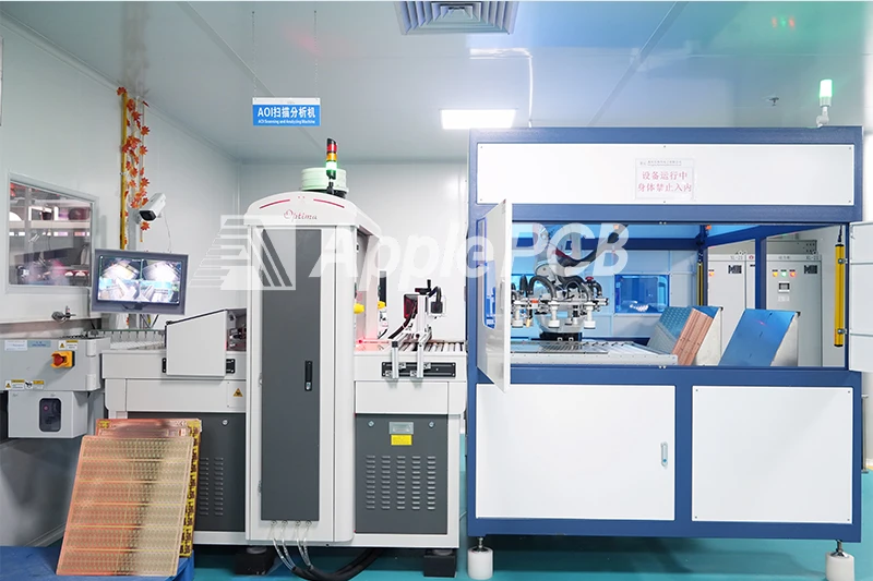
In the HDI PCB fabrication, the precise control of line width and line spacing is crucial. Due to the requirements of high-density interconnect, line width and line spacing must be very fine, usually below 4 mil. In addition, the location, thickness and bending angle of the line also have strict requirement because any small deviation will affect the electrical performance and signal integrity. However the LDI laser direct imaging used by ApplePCB can be a good solution to this problem, because it has more advantages than traditional contact imaging, and is able to deal with finer lines and graphics, which brings ApplePCB excellent line manufacturing capabilities.
| Copper Layer Manufacture Capacity | |
| Minimum Copper Pad for Laser Drill | Pad:5mil(laser drill 3mil) |
| (inner and outer layers) | Pad:6mil(laser drill 4mil) |
| Pad:8mil(laser drill6mil) | |
| Minimum Copper Ring for Via by Machine Drill | 4mil |
| (inner and outer layers) | |
| Min BGA Pad. | 8mil |
| Min Trace Width on BGA Area. | 2.5mil |
| Min Trace to BGA Pad Space. | 2.5mil |
| Min BGA Pad for HASL | 10mil |
| Min BGA Pad on Copper Plane Area for HASL | 12mil |
| Bonding IC Width/Space. | 3/3mil for plating gold, |
| 4/4mil for ENIG. | |
| Min Space Between Copper Plane. | 6mil |
| Minimum Trace Width/Space for Coil: | 1oz: 4/4mil |
| 2oz: 8/8mil | |
| 3oz:12/12mil | |
| Different Copper at One Core | 18/35um, |
| 35/70u, | |
| 70/105um, | |
| 35um/105um | |
| Machine Drill to Copper Space: | 4L-6L: 4mil; |
| 8L-12L: 5mil; | |
| 14L-18L:6mil, | |
| Laser Drill to Copper Space: | 4mil |
3. Difficulty of Inter-layer Connection
HDI multilayer PCB are wired with many layers and concentrated connections, so they require a large number of through-holes for connections. However, in order not to affect the stability of the line, we need to try to use blind, buried and microvias instead of traditional through-holes.
● Through-hole
Through holes are created by drilling through all the layers of the board from top to bottom. By coating them with copper they allow for the passage of currents. Through holes are considered the cost effective option, during manufacturing processes. However, because they need to penetrate the entire board, they take up more space, affecting the density of the wiring and the integrity of the signal, and therefore are not often found in HDI PCB.
● Microvias
Microvia refers to a particularly small hole that connects two layer, the common microvia size of 80-100 μm, a depth of 60-100 μm. Because the microvia are so small, they can be placed below the pads of fine-pitch BGA components/package, which greatly saves space on the PCB. Due to technological limitations, many HDI PCB manufacturers are unable to produce through holes in pads.
But ApplePCB adopts advanced laser drilling equipment, which can drill microvias with a diameter of 10μm(0.01mm). Some equipment can even drill hole from both side of the material at the same time, thus treating the thinner dielectric material before the lamination process, avoiding deviation that may be caused by one-sided drilling, and ensuring the accuracy and consistency of the hole.
● Blind Via and Buried Via
Blind via connect the outer layer of a PCB to one or more inner layers. Unlike through hole, they do not penetrate the entire board and are only visible on one side of the board. Buried via, on the other hand, are completely encapsulated in the PCB and connect two or more inner layers (usually for power and ground layers). Buried vias are not visible at both the top and bottom of the HDI PCB.
Blind and buried via are not only effective in reducing the number of layers and lowering production costs compared to through-holes. It also enables more and denser wiring by saving the location of through holes. This is very important for HDI PCBs. In addition, from an electrical point of view, blind and buried via also enable HDI boards to have better electrical performance and impedance control. So for greater benefit, HDI PCBs can be designed to minimize the use of through-holes and move to blind and buried vias instead, but this advantage comes at a price. Blind holes rely on high-precision laser drilling equipment, and buried holes are difficult and costly to produce.
How to Determine the Reliability of Blind Holes?
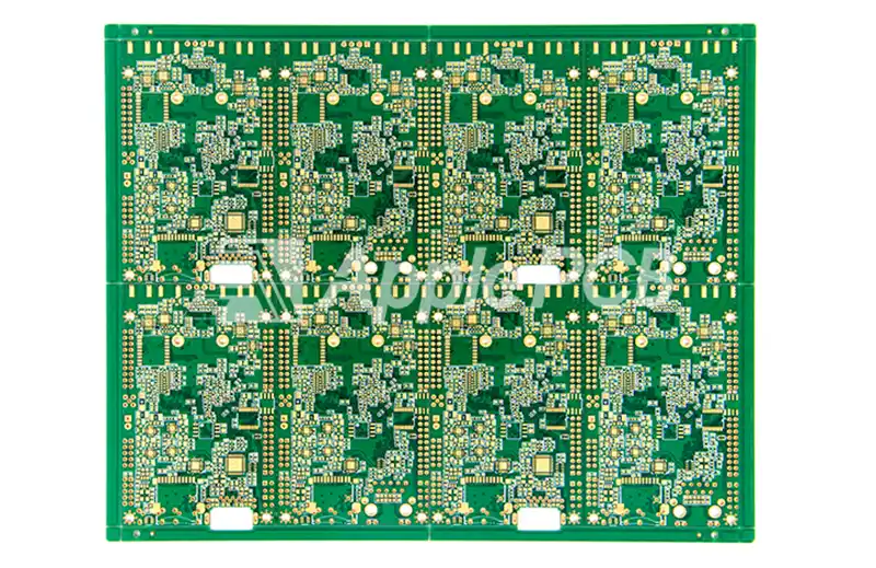
Since there are more laser micro vias in HDI boards, the reliability of laser blind vias directly affects the reliability of HDI PCBs. As a professional HDI manufacturer, we mainly judge from the two aspects of hole type and copper plating.
1. Hole Type:
(1) Plane Hole Type: By measuring the ratio of short diameter (a) and long diameter (b) to determine the true roundness. (General requirements for true roundness ≥ 90%). The formula is: true roundness = short diameter a / long diameter b * 100%
(2) Cross-section Hole Type: Cross-section hole type is more complex, mainly from the taper, hole wall roughness and the degree of copper damage to the substrate three angles of judgment. The cross-section hole pattern needs to be observed and measured by taking slices, but since grinding the slices may lead to changes in the hole pattern, these indicators are usually confirmed after copper plating.
● Taper:
Taper is determined by measuring the ratio of the lower hole size (b) to the upper hole size (a). (Taper ≥ 85% is generally required)
The formula is: Lower hole size b/upper hole size a*100%.
● Hole Wall Roughness
The hole wall roughness of blind holes is usually required to be ≤15μm, but may be adjusted according to the material or other factors.
● Degree of Substrate Copper Damage
The degree of substrate copper damage is generally required to be ≤1/3 of the substrate copper thickness.
2. Copper Plating Condition
We mainly analyze the copper plating condition of the holes from four indicators: corner copper thickness, dimple value, hole filling height, and hole wall copper thickness.
● Angular Copper Thickness
Corner copper thickness refers to the thinnest part of the plating. If the plating layer is too thin it can lead to HDI circuit boards electrical discontinuity or lack of durability. Hence it is important to maintain corner copper uniform and sufficient thickness by plating precisely to enhance the dependability of blind holes.
● Dimple Value
The dimple value is the depth of depression after filling, which represent the height difference between the filled copper layer and the initial copper layer. Ideally, there should be no visible depression after hole filling and the hole should remain flat. According to the IPC-A-600 standard, the dimple value is usually within ±76 μm. However, in order to improve the quality of soldering and the reliability of electrical connection, ApplePCB standard is more stringent, requiring a dimple value of ≤25μm.
● Hole Filling Height (Base Copper Thickness)
Hole filling height is similar to the copper thickness of the through-hole face, high-quality hole filling can improve the conductivity and thermal conductivity of the through-hole, to ensure the reliability of signal transmission and thermal management performance. ApplePCB's hole size for fill resin and copper-capped range is 0.15-0.5mm.
● Hole Wall Copper Thickness
Hole wall copper thickness refers to the thickness of the copper layer inside the via. It is similar to the copper plating thickness of through holes, but for HDI boards, especially microvias, a higher degree of precision and consistency is required. And Apple PCB utilizes state-of-the-art laser drilling equipment to ensure the quality of each microvia.
How to Choose the Right HDI PCB Manufacturer?
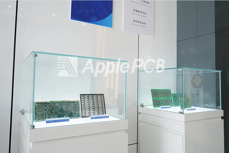
Due to the difficulty and high cost of HDI PCB manufacturing, the manufacturing capability of HDI PCB manufacturers and the cost of manufacturing are the primary considerations, in addition to customer service, delivery and quality control are also worthy of our attention.
1. Manufacturing Capability
As we mentioned in the previous article, the manufacturing difficulties of HDI PCB boards mainly lie in the blind embedded holes and high-precision line width and line spacing processing. ApplePCB has advanced technologies to perfectly handle these manufacturing difficulties:
●High-precision laser drilling machine: We employ cutting edge laser drilling machinery from Daqo Laser to meticulously regulate the size and depth of the microvia guaranteeing the quality and uniformity of each microvia.
●Advanced LDI technology: Utilizing our cutting edge Laser Direct Imaging (LDI) technology allows us to precisely make the line widths and spacings necessary, for HDI circuit designs.
2. Manufacturing Cost
Despite the high manufacturing cost of HDI PCB, ApplePCB offers competitive pricing through optimized production processes and economies of scale:
● Cost Optimization
With 90% automated equipment and an efficient production process, we can effectively reduce labor costs and production time. In addition, ApplePCB has a large-scale production capacity, through bulk purchasing and large-scale production, we can further reduce the cost of the single HDI PCB board so that we can provide customers with more favorable prices.
● Transparent Quotation
As we all know, some complex HDI PCB manufacturing projects need to add extra charges, such as line width and line spacing ≤ 0.127MM, over-hole ≤ 0.2MM ,half-hole boards, shaped, JB holes more than 2000, etc. ApplePCB will provide you with a detailed price break down based on your gerber information, including process costs, material costs, transportation costs. Meanwhile, we can also offer you competitive discounts for large quantity orders.
3. Customer Service
Quality customer service play a critical role in the smooth running of a project. Because the design document and manufacturing process of HDI PCB are more complex, timely communication with the HDI PCB supplier is required to minimize delays and errors and to speed up the project process. ApplePCB has a professional engineering team that can provide technical support such as design consulting, manufacturability analysis, etc. We can respond to customer inquirie and needs within 24 h to ensure that your problems are resolved promptly.
4. Quality Control
Quality control plays a role, in guaranteeing the performance and dependability of products. In specialized fields, like automotive and medical sectors where even minor flaws can have significant repercussions. Hence it is crucial to confirm that the chosen HDI PCB manufacturer possesses the quality certifications. ApplePCB has secured certifications to assure that our HDI PCBs adhere to quality benchmarks and satisfy the strict demands of the automotive and medical industries:
●IATF 16949:2024
●ISO 9001:2015
●ISO 13485:2016
●UL
5. Delivery Logistics
In a competitive market, fast delivery and stable logistics are very important. This helps to get products to market quickly, take the lead in the market, and ensure project advancement and quick turnaround of funds. ApplePCB has a strong production capacity, and is able to manufacture an average of 3,000m² of HDI PCBs a day through stable logistics channels (EMS, FedEx, DHL, etc.) we can complete the delivery of prototypes as fast as 3 days, and complete the delivery of bulk quantities in less than 1 week.
Of course, if it involves more complex HDI PCB manufacturing, this time may be extended, you can send us your specific design information in the lower right corner, we will provide you with a quote and estimated delivery time within 24h.
