In today's rapidly advancing electronics industry there is a noticeable shift, towards creating advanced devices that can handle increased currents and heat. This trend demands PCB that can handle higher electrical currents and more heat. Therefore, heavy copper printed circuit board (PCB) are being used to meet these demanding requirements.
What Is Heavy Copper PCB?
Printed circuit boards carry current through copper traces. To enhance the ability of a copper trace to carry current one option is to widen the copper wire, although this may not always be feasible. Another way to increase the current carrying capacity without changing the width of the copper traces is to use heavier or thicker copper.
A heavy copper PCB, also called thick copper PCB is a printed circuit board featuring 3 oz/ft²or more of copper on either inner or outer layer.
Why Do You Need Heavy Copper PCB?
The extra copper thickness allows the board to conduct more current and transmit signals across it, making them ideal for high current industries that require high power transmission, such as automotive and power supply electronics.
High Current
A significant benefit of heavy copper circuit board is the enhanced current-carrying capacity provided by the thicker copper layer, without compromising performance or causing overheating. This characteristic renders them exceptionally suitable for power electronic devices, which often necessitate currents exceeding 30 amps.
Applications: Power supplies, motor controllers and other high power devices.
High Heat Generation
Thicker copper layers lower the overall thermal resistance of the PCB, enabling heat to dissipate more easily. Therefor, the heat will have a larger copper surface for heat dissipation.
Applications: Heavy copper PCBs are extensively employed in automotive electronic systems, encompassing engine control units, powertrain systems and safety modules.
Space Constraints
Thick copper PCB can often accommodate higher currents with fewer layers compared to standard PCB, allowing for a more compact design and potentially decreasing the overall dimensions and weight of the PCB.
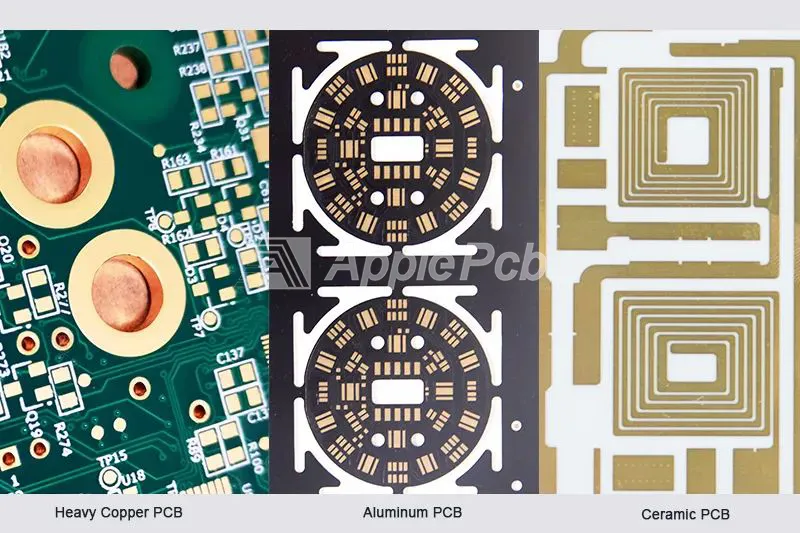
Heavy Copper, Aluminum and Ceramic PCB: A Comparison
Applications
Heavy Copper PCB: Specializing in applications that demand high power, high current and high frequency, Heavy Copper PCB are ideally suited for use in power supply units, motor control systems and RF amplification devices.
Aluminum PCB: Shines in applications demanding a balance of power, portability and weight. Like automotive electronics, aerospace components and portable devices.
Ceramic PCB: in high power, high heat and high frequency scenarios where superior thermal management is of the essence. This includes applications like LED lighting, military electronics and medical devices.
Manufacturing Difficulty
Heavy Copper PCB: The Heavy copper PCB fabrication necessitates complex lamination and plating techniques, thereby increasing complex of its manufacturing processes.
Aluminum PCB: The hardness of the material introduces substantial difficulties in drilling, milling and etching processes.
Ceramic PCB: The inherent brittleness and propensity for cracking in Ceramic PCB present significant challenges during the manufacturing process.
Material
Heavy Copper PCB: Central to the design of Heavy Copper PCB is an FR4 core, fortified with thick copper layers.
Aluminum PCB: The Aluminum PCB is characterized by an aluminum core, striking a balance between performance efficiency and weight.
Ceramic PCB: The Ceramic PCB utilizes a ceramic core (either aluminum Nitride or oxide), renowned for its superior thermal attributes.
Current Carrying Capacity
Heavy Copper PCB: Within this category, Heavy Copper PCB stands out for its exceptional ability to manage high currents, attributed to its substantial copper layer thickness.
Aluminum PCB: Exhibiting a moderate capacity for current conduction, Aluminum PCB serve well in applications with intermediate power requirements.
Ceramic PCB: In comparison, Ceramic PCB demonstrate a lower current carrying capacity, which limiting its use in high current applications.
Thermal Conductivity
Heavy Copper PCB: Renowned for their exceptional thermal conductivity, facilitating effective heat dissipation.
Aluminum PCB: Provide superior thermal conductivity when compared to FR4 PCB, rendering them highly suitable for applications with significant power requirements.
Ceramic PCB: Excel in thermal conductivity, surpassing that of Heavy Copper PCBs, thereby establishing them as the optimal choice for applications where heat management is crucial.
Weight
Heavy Copper PCB: Possesses the greatest weight among the trio, attributable to its densely layered copper construction.
Aluminum PCB: Aluminum circuit boards are lighter than heavy copper PCB but still weigh more, than FR4 circuit boards.
Ceramic PCB: Achieve an optimal equilibrium between weight and performance characteristics, presenting a reduced weight advantage over Heavy Copper PCB, However, it is close to the weight of FR4 PCB.
Choosing the Appropriate Copper Thickness
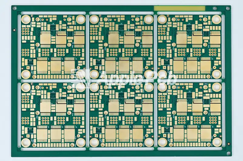
Thicker copper can handle higher currents and dissipate heat better, but may increase cost and manufacturing difficulty. It also impacts signal integrity in high frequency applications and overall board weight. The right thickness balances electrical performance, reliability, cost, and manufacturability.
Copper Weight and Thickness
The weight of copper is gauged in terms of ounces per square foot (oz/ft²). Such as, should 1oz of copper be evenly spread to envelop a surface area of 1 square foot, it would result in a thickness of 1.4 mils.
The below table shows copper weight versus copper thickness in mils.
| Copper weight | Approximate thickness in mils | Approximate thickness in µm |
| 1 oz copper PCB | 1.4 mils | 35 µm |
| 2 oz copper PCB | 2.8 mils | 70 µm |
| 3 oz copper PCB | 4.2 mils | 105 µm |
| 4 oz copper PCB | 5.6 mils | 140 µm |
| 5 oz copper PCB | 7 mils | 175 µm |
Copper Thickness for Different Applications
| Copper Thickness (oz/ft² / µm) | Typical Applications |
| <1 oz / <35 µm | Low-power electronics (sensors, simple circuits) |
| 1-2 oz / 35-70 µm | Standard PCB (various applications) |
| 3-6 oz / 140-210 µm | Heavy copper PCB (industrial applications, high power LED modules, power supplies) |
| 6-10 oz / 210-350 µm | Very specialized applications (high power industrial equipment, motor drives) |
| >10 oz / >350 µm | Extremely rare and custom applications (Power distribution, military, aerospace) |
Calculate the Copper Thickness According to Current
When deciding on the right copper thickness for your PCB you need to take into account how current the copper traces can carry. This can be figure by adhering to the IPC2221 standard. This standard provide a computational formula to identify the cross sectional area of the trace, contingent on the specific current it is designed to bear. The formula is as follow:

where:
I is the current in amperes
Inner layers: k = 0.024
Outer layer: k = 0.048
b = 0.44, c = 0.725
k, b, and c are constants derived from curve fitting the IPC-2221 curve
TRise is the temperature rise above the ambient temperature in degrees Celsius
A is the cross-sectional area of the trace in square mils.
Disclaimer:
The IPC-2221 data from which these formulas are derived only covers up to 35 Amps, trace width up to 400 mils, allowable temperature rise from 10 to 100 degrees Celsius, and copper of 0.5 to 3 ounces per square foot. If used outside of these ranges, this calculator will extrapolate thus becoming more inaccurate with higher currents.
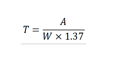
Final, to determine the thickness of copper traces (T) in mils you should divide by the width of the traces (W). A rough estimate is that 1 oz/ft² equals around 1.37 mils so dividing, by 1.37 will convert mils to oz/ft²:
Consult with ApplePCB
The ideal copper thickness ultimately depends on the specific needs of your application. Consider factors like current requirement, heat dissipation need, signal integrity (for high frequency applications), and mechanical strength. ApplePCB offer professional guidance tailored to customer designs, such as appropriate copper trace width and thickness, to ensure the desired performance.
How to Design Heavy Copper PCB?
Heavy copper PCB are highly valued for their excellent heat dissipation and enhanced current carrying capabilities. Designing these boards requires meticulous planning to optimize their performance and address potential challenges.
Managing Thermal Dissipation
Since heavy copper PCB has good thermal conductivity, the heat dissipation method should be designed reasonably. The heat dissipation effect can be improved by:
Using larger copper pour areas connected to heat sources helps spread and dissipate heat more effectively.
Integrating thermal vias is a key strategy. These vias create efficient heat paths from the top to the bottom layers of the PCB.
Ensuring adequate spacing between components facilitates better airflow and natural cooling.
Using of heat sinks or thermal pads for components that generate significant heat can further enhance cooling.
Thermal Expansion
The substantial thermal conductivity of thick copper PCB can result in non-uniform heat dissemination across components and solder joints. This irregular heat transfer can generate significant temperature variances, prompting the PCB to expand and possibly distort. It's crucial to ensure appropriate spacing and meticulously plan the arrangement of components and solder joints to avert stress induced by thermal effects.
Electrical Performance
The presence of thick copper layers can considerably affect the electrical properties of the PCB, encompassing impedance, capacitance and inductance. To counter these impacts, meticulous modeling and simulation are necessitated to comprehend how these alterations affect signal integrity and power distribution.
Trace Width and Spacing
Due to the good electrical conductivity of thick copper, the trace width and trace space can be appropriately increased, while avoiding excessively long traces to reduce signal attenuation and interference.
Copper Plating Method for Making Heavy Copper PCB
The PCB laminate, pre-clad with copper on both sides are procured directly from the laminate provider. The laminate appears as a solid copper sheet. This pre-clad laminate is available in a range of copper thicknesses, enabling the manufacturing of PCB circuit board with varying thicknesses and final copper weight. Thick copper PCB fabrication has primarily two methods for copper plating.
Chemical Copper Plating
Chemical copper plating is prevalently employed in the fabrication of circuit boards with through holes, and it doesn't necessitate an external power source. The primary objective of this method is to deposit a copper layer on a non-conductive substrate via a sequence of chemical processes. This layer is then thickened through subsequent electroplating to achieve a specific design thickness, typically 1 mil (25.4um) or more. Sometimes, the copper thickness is even directly deposited through chemical copper plating.
Electroplating
Electroplating works well for creating exceptionally thick copper layers. In the procedure a solution containing copper sulfate, sulfuric acid and chloride ions is used. By applying current the copper ions from the electrolyte are deposited, forming a dense copper layer on the surface of the PCB.
Difficulties of Manufacturing Heavy Copper PCB
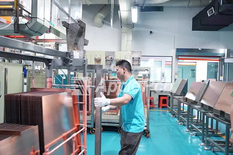
1. Etching
Challenges:
Difficulty in Chemical Exchange: As the copper thickness increases, it becomes harder for etching chemicals to evenly interact with the surface. This leads to significant side etching (undercutting), where the chemical removes more material horizontally than vertically.
Controlling Side Etching: The goal is to minimize side etching to maintain the desired pattern accuracy.
Strategies:
Stepwise Fast Etching: Implementing multiple quick etching steps rather than a single prolonged process helps reduce the side etching in each step.
Etching Compensation Factors: Increasing the compensation factors during the design phase allows for anticipating and countering side etching, ensuring precise final pattern dimensions.
2. Lamination
Challenges:
Increased Risk of Slippage: The use of more prepreg (semi-cured resin sheets) as copper thickness increases can lead to misalignment or "slippage" during lamination.
Filling of Void Areas: Large blank areas in thick copper PCBs can form voids or uneven surfaces during lamination.
Strategies:
Use of Fillers: Employing silicone and resin to fill the gaps in blank areas between patterns helps to avoid slippage and void formation.
Choosing Appropriate Materials: Selecting materials with a low CTE (Coefficient of Thermal Expansion) and high Td (Decomposition Temperature) is essential for maintaining the quality and reliability of thick copper PCBs.
Extending High-Temperature Lamination: Increasing the duration of the high-temperature phase during lamination ensures complete curing of the prepreg, preventing issues like resin under-curing, which can compromise the board's reliability.
3. Drilling
Challenges:
Increased Board Thickness: As the copper thickness increases, the overall PCB thickness also increases, making the drilling process more challenging.
Drilling Quality Issues: Drilling thick copper boards can lead to problems like rough hole walls or uneven hole diameters.
Strategies:
Using New Drill Bits: Employing new drill bits can minimize wear and ensure higher quality holes.
Segmented Drilling: Using a segmented or step-drilling approach can reduce the load and heat accumulation on the drill bit.
Optimizing Drilling Parameters: Adjusting parameters such as feed rate and retract speed can improve the drilling quality, reducing roughness and maintaining accurate hole diameters.
Precision Drilling in ApplePCB
At ApplePCB, we are equipped with top tier automated drilling instruments and avant garde laser drilling technology. This distinct combination empowers us to fulfill the needs associated with diverse types and designs of PCB.
Why Choose ApplePCB?
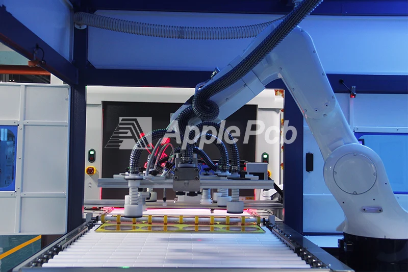
Advanced Production Capabilities
ApplePCB is a reliable heavy copper PCB supplier. With our experience and resources we can produce PCB featuring inner layer copper thickness ranging from 0.5oz to 12oz and outer layer copper thickness from 3oz to 20oz.
| Feature | Capability |
| Material | FR4, aluminum |
| Min. Trace Width/Space | For outer (finish copper): |
| 4oz Cu 10mil/13mil,5oz Cu 12mil/15mil | |
| 6oz Cu 15mil/15mil,12oz Cu 20mil/32mil | |
| ............................................................................... | |
| For inner (finish copper): | |
| 4oz Cu 8mil/8mil,5oz Cu 10mil/10mil | |
| Max Layers | 10L (heavy copper). |
| Min. Hole Size | 8mil |
| pcb thickness/hole size ratio | Maximum:12:1 |
| Max PCB Size | 1200*500mm |
| Max Outer Layer Copper Weight (Finished) | 20oz |
| Max Inner Layer Copper Weight | 12oz |
| Board Thickness | 0.2-8mm |
| Surface Finishing | OSP, HASL lead free, Hard Gold (Electrolytic Gold), Immersion gold, Immersion Tin, Immersion Silver, ENEPIG |
| Solder Mask | Green, Red, Yellow, Blue, White, Black, Purple, Matte Black, Matte green |
| Silkscreen | White, Black |
| Via Process | Tenting Vias, Plugged Vias, Vias not covered |
| Test | Fly Probe Testing (Free) and A.O.I. testing |
| Build time | 5-10 days |
| Lead time | 2-3 days |
Adequate Testing Equipment
As a thick copper PCB manufacturer, ApplePCB has introduced advanced copper thickness testers, inductance measurement instruments, and micro-resistance measurement devices to ensure the highest quality and performance of our thick copper PCB.
Advanced Manufacturing and Test Processes
We employ an extensive electroplating process, lasting up to 70 minutes, to achieve a consistent and robust copper thickness. After copper deposition, backlight test is performed to ensure the adhesion of hole copper. After etching, slice analysis is performed to ensure the thickness of hole copper and surface copper. AOI optical scanning ensures the straight-through rate of the circuit (preventing open circuit, short circuit, fine line breaks, etc.). High speed screw flying probe machine test ensures the yield rate of the board. The solder mask is exposed by LED parallel exposure machine, and the exposure uniformity is more than 90%. High-precision laser text printing ensures the clarity and accuracy of the text on the PCB.
Premium Materials
What distinguishes us from heavy copper PCB manufacturer is that our PCBs are manufactured using A-grade laminates from renowned suppliers like Shengyi and Kingboard (KB), meeting UL and RoHS standards.
FAQs about Heavy Copper PCB
How much space should be left between copper features?
In PCB design its advised to increase the distance between copper components. Etching the gaps between traces is tougher, than etching a trace of the width.
| Cu Weight | Min Recommended Space between Copper Features |
| 1 oz | 3.5 mil (0.089 mm) |
| 2 oz | 8 mil (0.203 mm) |
| 3 oz | 10 mil (0.254 mm) |
| 4 oz | 14 mil (0.355 mm) |
Can standard PCB lamination techniques be used with heavy copper PCB?
Yes, standard PCB lamination techniques can be used to safely sandwich up to 50 layers of copper windings as thick as 10 oz/ft2. But with careful process adjustments in lamination and solder mask.
What kind of laminate used to manufacture heavy copper PCB?
High TG FR4 or ceramic-based laminates are designed to withstand higher temperatures, making them suitable for applications with high power densities and heat generation.
What are some alternatives to heavy copper PCB?
Aluminum PCB: while being lighter than heavy copper PCB and exhibiting decent heat conductivity, have a somewhat constrained current carrying capacity.
Ceramic PCB: known for their superior thermal conductivity, can handle exceptionally high current, albeit at a premium cost.
What are the disadvantages of heavy copper PCB?
Increased cost: The necessity for specialized manufacturing procedures and materials for heavy copper escalates their cost, rendering them pricier than standard PCB.
Manufacturing complexities: The processes of lamination, etching and drilling of thick copper can present increased intricacies.
Weight: Owing to the augmented quantity of copper, heavy copper PCB exhibit a greater weight compared to standard PCB. This could potentially be a consideration for applications that are sensitive to weight.
Impedance control: Achieving precise impedance matching can be more challenging due to the thicker copper layers.
