With the rapid development in the field of high technology, High Frequency PCB (HF PCB) gradually becomes the focus. High Frequency PCBs show their irreplaceable and critical role in the rapid transmission of 5G signals, precise detection of radar systems, and high-definition imaging of medical equipment. They are capable of handling higher frequency signals that are difficult to cope with by ordinary PCBs, and represent the trend and direction of future technology development. So ApplePCB has been closely watching and actively learning the most cutting-edge manufacturing technology of High Frequency PCBs board, and is committed to providing customers with the best solutions.
What is a High Frequency PCB?
In the frequency domain, signals are defined by the time it takes to complete a cycle through them. High Frequency PCBs are "high" in the sense that the circuit board signals vary at a certain rate, making signal integrity significantly affected by impedance and other circuit board parameters. So how high is high? For RF signals, it means signal frequencies above 50MHz. Signals above this range change very quickly, so it is necessary to use a suitable High Frequency PCB to ensure signal integrity.
The Difference Between High Frequency and High Speed PCBs
When discussing high frequency circuit board, people often associate them with High Speed PCBs, however, in fact, High Frequency and High Speed are not directly related. They as two completely different concepts can be applied simultaneously or separately in circuit board design. Whether it is a separate High Frequency PCB, High Speed PCB, or a PCB with both High Frequency and High Speed characteristics, ApplePCB has a wealth of manufacturing experience. Here are some of the key differences:
1. Main Concepts
High-speed PCBs are boards that are capable of receiving or processing digital signals at high speeds (measured in bits/second or bytes/second). Generally speaking, when the ratio of signal transmission time to rise time is greater than 1, we can consider the signal transmission to be high-speed.
High Frequency PCB refers to a circuit board that is capable of propagating analog or RF signals at high frequencies (in s-1 or Hz). As we mentioned earlier, generally 50MHz or more can be referred to as a high frequency signal.
2. Material
High-frequency printed circuit boards often use specialized laminates, such as Rogers or Taconic, which can effectively reduce signal loss and ensure high-quality signal transmission but more expensive. On the other hand, high speed PCB often use traditional FR-4 laminate, which are suitable for general fast digital signal transmission need.
3. Design Issues
During the design process, high Frequency PCB require special attention to signal loss, impedance matching, crosstalk and other issues. These issues directly affect the quality and stability of high-frequency signal transmission. The design of high-speed printed circuit boards need to pay attention to the correct termination alignment to avoid signal reflection problems, to ensure signal integrity and stability.
Types of High Frequency PCBs
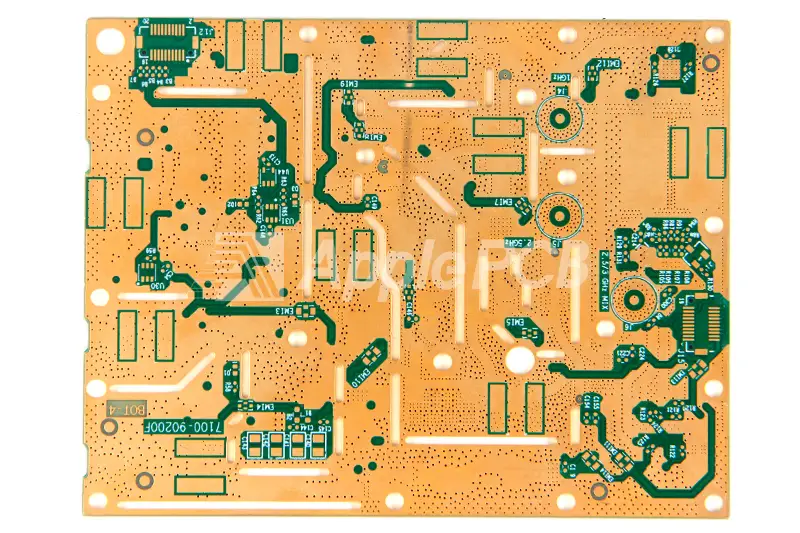
Due to the different classification standards, High Frequency PCB has many classifications. According to which we can have a more comprehensive understanding of High Frequency PCB.
1. Classification by Material
●Organic materials: phenolic resin, glass fiber/epoxy resin, polyimide (Polyimide), BT/Epoxy, etc. These materials usually have good electrical and mechanical properties.
●Inorganic materials: such as aluminum, Copper-Invar-Copper, ceramics, etc. These materials have excellent heat dissipation.
2. Categorized by Rigid and Flexible
●Rigid PCBs: Rigid High Frequency PCBs, commonly used in applications that require rigid support.
●Flexible PCB: Flexible High Frequency PCB, suitable for application scenarios that require bending and folding.
●Rigid-Flex PCB: Combines the advantages of both rigid and flexible PCBs and is suitable for more complex electronic devices.
3. Categorized by RF Signals
●RF 6-24GHz PCB: Capable of transmitting and receiving RF signals from 6 to 24GHz.
●RF 77GHz PCB: Capable of transmitting and receiving RF signals up to 77GHz, suitable for locating objects at long distances.
●Antenna Embedded PCB: This High Frequency PCB is developed from the RF 77GHz PCB with smaller conductor width, conductor spacing, conductor tolerance and rounded corners.
4. Categorized by Application
●Communication equipment: Network equipment, signal measurement equipment, etc.
●Data processing and storage: Backplanes, servers, etc.
●Automotive and transportation: Radar and sensors for automobiles, etc.
●Aerospace and military: Aviation communication and navigation systems, military radars, etc.
●Communication infrastructure: Cellular base stations, satellite communications, wireless links, etc.
Why are High Frequency PCBs more Expensive?
High frequency circuit boards tend to be pricier than PCBs due to the need for costlier base materials and a more intricate design and manufacturing process.
Materials like PTFE ceramics and ceramic filled substances found in high frequency PCBs provide performance guaranteeing signal transmission with minimal loss. However this enhancement comes at the expense of material costs.
When designing, in order to ensure the stable performance of High Frequency PCB, it is necessary to calculate impedance more accurately, design thermal management, etc, which also invariably increases the cost of design.
The production of High Frequency PCBs is notably more intricate than that of PCBs demanding manufacturing with strict tolerances to uphold the integrity of the High Frequency signal. This also calls for manufacturers to possess advanced production methods and equipment necessitating a specific level of investment costs.
How to Select High Frequency PCB Materials?
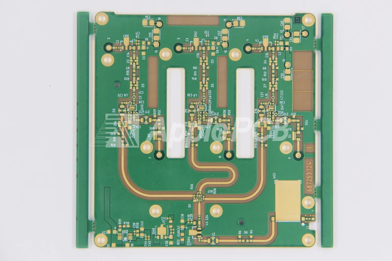
When we choose HF materials it's important to think about more than the Dk and Df values. We should also take into account the mechanical characteristics of the material well as factors like thickness, size and the type of copper foil.
Characteristics of Laminate
1. Small RF Circuit
If you aim to create a very small RF printed circuit, opt for materials with a large real part of the dielectric constant (Dk). This is because a higher Dk value reduces the signal wavelength allowing for a compact circuit design.
2. Low Loss Circuit
When aiming for loss in a circuit, opt for a material with a dielectric constant imaginary part (Df). This is because a lower Df value helps retain signal integrity by minimizing signal loss during transmission.
3. Long Distance Interconnection
If the circuit is designed with long interconnection where there is a risk of excessive loss, then materials with a lower Df should also be selected. This reduces signal loss over long distances.
4. Harsh Environments
If your High Frequency PCB in the application may experience high temperature, thermal cycling, vibration and shock and other harsh environments, then you need to consider the reliability of the material from the Tg, Td, Z-CTE, T288, water absorption and other characteristics.
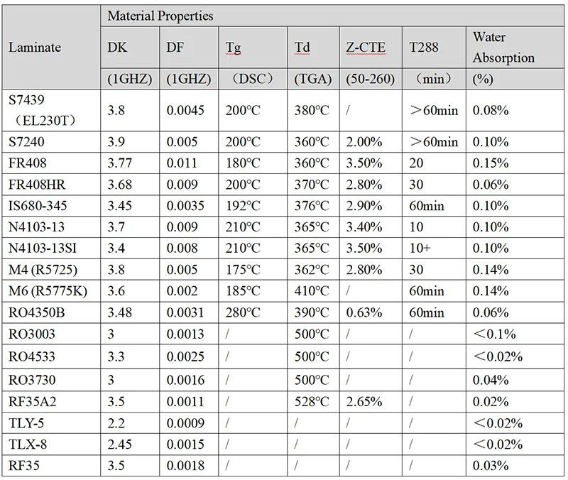
In the table we listed ApplePCB standing high-frequency laminate and their characteristics. Of course, this is only a small part of the high-frequency plate is very much more, if you still want to know more about the characteristics of the Laminate, you can contact us in the lower right corner, our professional engineers will be for you to free answer.
5. Electric Field
Another factor that deserves our attention is the direction of the electric field, since the dielectric constant of the Laminate material is different in each axis of the material, which may affect the speed of signal propagation and resonance. Although these differences may only be about 5%, but this is important in RF printed circuits that rely on resonance such as wave guides, antennas and resonators. You can contact us in the lower right corner to obtain material data on dielectric constant values for different polarization directions for your high frequency PCB board.
Thickness and Size
High Frequency PCB material are usually available in specific thicknesses and panel sizes, and the high frequency PCB manufacturer will make cutouts as well as layer combinations to achieve the desired size and final thickness. For High Frequency PCBs, the thickness of the substrate is very important as it will determine the line width required for the impedance of the target system. Typically smaller circuit size design require thinner laminates to accomplish.
Copper Foil
In general, choosing a copper foil with less RMS roughness reduce signal loss and interference. ApplePCB can provide you with different types of copper foils to meet your different needs.
| Copper Foil Type | Roughness |
| Electro deposited | above 1 um |
| RTF | 0.5 um to 1.5 um |
| Rolled-annealed | 0.25 to 0.5 um |
| Ultra-low Profile | can be less than 0.3 um |
If you need to evaluate the conductor loss of High Frequency PCB materials, ApplePCB advise you to use trace's DC resistance, skin effect, and copper roughness factor to estimate the conductor loss:

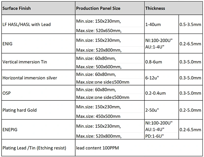
In addition to RMS roughness, we also need to consider the plating material of the copper layer, as these materials may introduce rough surface and producing greater loss. If your device operates above 2.4 GHz WiFi or has a long interconnect length, then ApplePCB recommends that you use OSP or ImAg plating as they add little to no additional loss. Below is a list of surface treatments that ApplePCB can provide:
Noteworthy Issues in High Frequency PCB Design
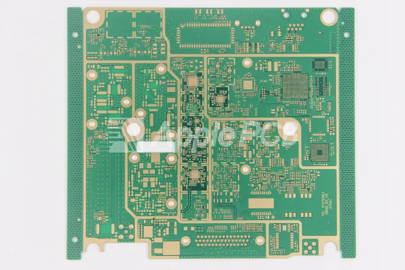
When designing high-frequency circuit board, special attention can be paid to the following area to avoid issue. This will avoid additional time costs and facilitate a silky smooth transition from design to manufacturing.
1. Avoid high-frequency interference: You can reduce crosstalk by increasing the distance between the high-speed signal and the analog signal. Of course, we should also pay attention to the digital ground to analog ground noise interference.
2. To realize the differential distribution line: The differential distribution line needs two lines of the same length, and the spacing between the two lines remains constant, which is determined by the differential impedance. There are two ways to parallel alignment: one is the two lines in the same layer, the other is the two lines in the neighboring upper and lower layers.
3. Matching resistor for differential pairs at the receiving end: Usually a matching resistor is added between the differential pairs at the receiving end, the value of which should be equal to the value of differential impedance in order to improve the signal quality.
4. Transmission line design: In High Frequency PCB design, the design of controlled impedance transmission lines is critical to avoid signal loss. Common methods are microstrip lines and ribbon lines.
● Microstrip lines: These are traces with a ground plane in the outer layer. Its impedance calculation is complex.
● Ribbon line: Similar to microstrip line, but with an additional grounding layer at the top of the trace, which provides better impedance control and reduces EMI radiation. Besides,Adopt 45°angle of transmission line corners to can reduce return loss.
5. Avoid leaded components: High frequency environment should avoid the use of components with leads, recommended the use of surface mount components to reduce the tap inductance.
6. Select plating process: Select OSP or ImAg process instead of HASL method to improve the skin effect of high-frequency current and reduce environmental pollution.
7. Provide rich grounding layer: Use molded holes to connect the grounding layer to prevent the impact of three-dimensional electromagnetic fields on the high frequency circuit board.
8. Deal with theoretical and practical wiring conflicts: High-speed wiring and EMI requirements may be in conflict, by adjusting the alignment and PCB stacking to reduce EMI problems, such as high-speed signals to the inner layer.
Problems to Be Aware of When Producing High Frequency PCBs
Transmission Line Manufacturing Accuracy
High-frequency signal transmission requires extremely high manufacturing accuracy for transmission lines, generally within±0.02mm. ApplePCB's accuracy is generally controlled at ±0.01mm, and at the same time ensure that the edges of the transmission line are very flat, no burrs or gaps are allowed to meet the stringent requirements of high-frequency signal transmission. Through the following table you can have a clearer understanding of our High Frequency PCB circuit manufacturing capabilities:
| Items | Abilities |
| Min BGA pad. | 8mil |
| Min Trace Width on BGA Area | 2.5mil |
| Min Trace to BGA Pad Space | 2.5mil |
| Bonding IC Width/Space | 3/3mil for plating gold, |
| 4/4mil for ENIG. | |
| Min Space Between Copper Plane | 6mil |
| Minimum Trace Width/Space for Coil | 1oz: 4/4mil |
| 2oz: 8/8mil | |
| 3oz:12/12mil | |
| Different Copper at One Core | 18/35um, 35/70um, 70/105um,35um/105um; |
| Machine Drill to Copper Space: | 4L-6L: 4mil; |
| 8L-12L: 5mil; |
Plating Thickness Control
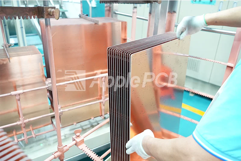
The characteristic impedance of the transmission line directly affects the transmission quality of microwave signals, and the characteristic impedance is closely related to the thickness of the copper foil, especially for the hole metallization of the microwave board, so the uniformity and control of the plating thickness is particularly important. ApplePCB uses precision thickness detection equipment and fully automatic plating process in the plating thickness control, which ensures the uniformity and stability of the plating.
Characteristic Impedance Control
Characteristic impedance is one of the core requirements of high frequency microwave boards, products that cannot meet the requirements of characteristic impedance will not work properly. Therefore, it is necessary to use appropriate lamination parameters and pressure during the lamination process, so as to ensure the consistency of the layer and the stability of the dielectric properties.
Drilling quality control
Different dielectric materials have specific requirements for drilling parameters, top angle of the drill, edge length, helix angle, etc. ApplePCB has developed detailed drilling process parameters for different materials and uses high-precision Mitsubishi laser drilling equipment, which can avoid generating rough edges that may lead to distortion of signals, and ensures good electrical performance of the product at high frequencies.
Mechanical Processes
Since different high frequency dielectric materials have different characteristics, different opening and forming processes are required. The traditional printed circuit board under the material are usually shearing machine or semi-automatic opening machine, but for high-frequency microwave board media materials, these methods are not always applicable.
ApplePCB will be based on the material characteristics of the most suitable process (milling/cutting-based), to avoid deformation of the material and the surface quality of the problem, so as to ensure the accuracy of the processing and Laminate the consistency of the material. Different milling parameters need to be set for different materials in the molding process. For example, when it comes to Laminate, we usually use neutral coolant for cooling during the milling process to prevent material overheating and deformation.
High Frequency PCB requires much higher machining accuracy than traditional PCB, usually the shape tolerance needs to be controlled within ±0.13mm, but through the high-precision CNC milling and cutting equipment, as well as a wealth of experience in processing, ApplePCB can minimize the shape tolerance needs to be controlled within ±0.05mm.
Our High Frequency PCB Fabrication Capacity
| Item | Parameter |
| Layer Count | 1-40L |
| Mixed Stack up | FR4+High frequency |
| PCB Thickness | 0.2-8mm |
| Thickness Tolerance | ≤1.0mm: +/-0.10mm, |
| >1.0mm:+/-10%. | |
| Minimum PCB Size | 2.5x2.5mm need create panel, |
| 10x10mm can do single board. | |
| Minimum PCB Size | 500x1200mm |
| Maximum Copper | 3oz |
| Normal Lead Time | 4-6 Working Days |
| Fast Lead Time | 1-2 Working Days |
| Materials | Rogers,ISOLA, Shengyi, Nelco, Arlon etc. |
| Qualifications | IATF 16949:2024 |
| ISO 9001:2015 | |
| ISO 13485:2016 | |
| UL |
Choose ApplePCB as Your High Frequency PCB Manufacturer!
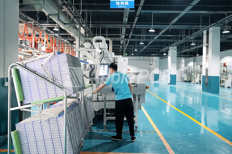
We all know that High Frequency PCB require more advanced design and manufacturing technique than regular PCB, and ApplePCB is a trusted High Frequency PCB manufacturer with over 15 year of experience and proficiency in advanced Laser Direct Imaging (LDI) and Controlled Impedance Drilling (CID) technique. Our high-frequency PCB factory is equipped with state-of-the-art han's laser equipment and fully automated production lines. In addition, we have long-term relationship with several well-known material supplier and a large and stable inventory of high frequency material, including Rogers material, PTFE, ceramic-filled PTFE, CE, and FR4+PPO, etc.
ApplePCB's customer support team is ready to assist you in ensuring that your project runs smoothly. Don't hesitate to contact us in the lower right corner to get started on your High Frequency PCB project.
