High-speed PCBs are the workhorses of modern electronic, enabling high performance data transmission and reliable signal integrity in applications like computer motherboard, advanced mobile devices, and high speed networking equipment. As signal frequencies continue to climb, engineers face challenge in ensuring signal integrity and minimizing noise. This article will explore the complexities of high speed PCB design and the latest material used to overcome these challenges.
What Are High-Speed PCBs?
High speed PCBs are specifically designed to handle electronic signal traveling at high frequency, typically exceeding 1 GHz, between 3-25 Gbps. Unlike standard PCB, where signal integrity might be less critical, high speed PCBs require extremely precise control over a property called impedance.
What Is Impedance in PCB?
Impedance extends the concept of resistance to alternating current (AC) circuits and includes not only resistance but also reactance, which accounts for the effects of capacitors and inductors. Impedance is frequency-dependent and also measured in ohms (Ω).
Inconsistent or uncontrolled impedance is like having potholes on a highway for data. It disrupts the flow of signals, causing them to reflections, attenuation, and crosstalk, leading to distorted and unreliable data transmission of your electronic device.
Benefits of High-Speed PCBs
Reduced Signal Distortion
By minimizing signal distortion and crosstalk, high-speed PCBs enable faster data transfer rates. This allows for faster processing and quicker response times.
Improved Signal Integrity
Consistent impedance ensures clear and undistorted signals and leads to more accurate data processing and reduced errors.
Reduced EMI/RFI
Precise impedance control helps minimize electromagnetic and radio frequency interference. This ensures reliable operation in environments where potential noise sources exist, preventing signal disruptions.
When Do You Need High-Speed PCBs?
Whenever you deal with electronic circuits that operate at high frequency and require clean, undistorted signal transmission, high speed PCBs become necessary. Here are some key situations where high speed PCB circuit boards are employed.
High-Speed Digital Applications
● DDR memory: High speed memory interface for data transfer within computer and embedded system.
● High-speed Ethernet (10 Gbps and above): Networking equipment transmitting large amount of data at high speed.
● USB 3.0 and newer version need fast signal transmission for data transfer efficiently between devices.
● PCI Express (PCIe): High-bandwidth interconnection standard for connecting various components within a computer system.
RF (Radio Frequency) Circuits
● Wireless communication devices: Cell phones, Wi-Fi routers, Bluetooth modules.
● Radar systems: Transmit and receive radio waves to detect objects.
● Microwave circuits: Used in various applications like heating food and satellite communication.
High-Precision Analog Circuits
● High speed data converter: Analog-to-digital and digital-to-analog converter used in various applications like audio processing and data acquisition.
● High frequency amplifier: Used to boost the strength of weak signal.
Planning High-Speed PCB Impedance
Dielectric Constant of Materials
The dielectric constant of the PCB material greatly affects the characteristic impedance of the signal trace. A lower Dk lead to a higher characteristic impedance for a given trace width and spacing.
Stack-Up Design
The arrangement of layers in a high-speed PCB, plays a critical role in controlling impedance. Different materials with specific dielectric constants (Dk) are used in each layer. By carefully calculating the thickness and arrangement of these layers, designers create a controlled environment for signal propagation.
Trace Geometry
The width and thickness of copper traces significantly impact impedance. Wider and thicker traces on a PCB have lower impedance, allowing signals to travel more easily. Designers meticulously calculate trace dimensions based on the target impedance and material properties.
Via Placement and Routing
Vias (connection points between layers) can introduce unwanted inductance and capacitance. Careful via placement and routing strategies minimize these effects and maintain consistent impedance.
Advanced Techniques
Advanced techniques like Controlled Depth Impedence (CDI) is employed, for extremely high-speed applications. CDI involves embedding the trace within a dielectric layer for even more precise control.
Planning High-Speed PCB Stackup
The positioning of power, ground, and signal layers within the stackup can greatly influence cross-talk, electromagnetic compatibility (EMC), and trace routing, helps to provide a stable, low-impedance reference for the high-speed signals.
Power and Ground Planes
Power and ground planes should be positioned in close proximity to the signal layers to provide a low-impedance reference and return path for the high speed signals. As we know that the power and ground planes are placed on adjacent inner layers, with the signal layers sandwiched between them.
This configuration offers several benefits:
● Maintains a consistent characteristic impedance for the traces.
● Reduces crosstalk and electromagnetic interference (EMI) between signal traces.
● Provides a stable power distribution throughout the design.
Signal Layers
The signal layers should be positioned between the power and ground planes to take advantage of the controlled impedance environment. This arrangement helps to minimize signal reflection, ensure uniform propagation delay, and improve signal integrity. In addtion, depending on the number of required signal layer, the signal layer can be distributed throughout sections of the stackup. For instance, in a multilayer PCB high speed signals are usually positioned closer to the center of the stack, whereas slower signal can be routed on the outer layer.
Layer Spacing
The spacing between the power/ground plane and the signal layers is also an important consideration. Maintaining a closer spacing between the signal layer and the power/ground plane, can ensure a consistent and controlled impedance, reduce the risk of signal reflection and impedance mismatches, but it is limited by manufacturing constraints or dielectric thickness requirement.
Check Our Capabilities
| Item | Capability |
| Layers | 4-40 layers |
| Materials | Low loss/low Dk, high-performance FR-4, PPO, Teflon, hydrocarbon/ceramic filled |
| Minimum Trace width /Spacing | 2.5/2.5mil |
| Maximum Panel Size | 580mm x 1010mm |
| Surface Finish | plating NI/AU, plating hard Gold, ENIG, Immersion Tin, Immersion silver, OSP, ENIG+OSP |
| Aspect Ratio | Maximum 12:1 for plated through holes |
| Copper Thickness | Up to 12 oz on both sides |
| Solder Mask Thickness | Minimum 50μm |
| Routing Dielectric Thickness | 0.1mm - 3.0mm |
| Impedance | Minimum control of 50 ohms +/- 5 ohms |
| Drilling | Minimum mechanical drill diameter 0.15mm |
| Minimum laser drill diameter 0.075mm | |
| Lead time | 7-15 business days |
| Certification | UL, RoHS, ISO 9001,ISO 13485, IATF 16949 |
| IPC Standard | IPC2141 |
High-Speed PCB Design Guidelines
1. Define Requirements
Target Impedance: Determine the desired impedance value for your signal paths based on the operating frequency and desired signal characteristics.
Material Selection: Choose materials with appropriate dielectric constants (Dk) and loss tangents (Df) to achieve the target impedance and minimize signal loss. High-performance materials like Rogers are often used for HSPCBs.
Number of Layers: A higher layer count allows adding ground planes, interplane layers, and power planes to maintain electromagnetic compatibility, for better signal routing and isolation but increases complexity and cost.
2. Layer Stackup Design
Power/Ground Planes: Dedicate at least one inner layer for a continuous ground plane to provide a reference for signal return paths and minimize noise. Additional power planes might be needed depending on power requirements.
Controlled Impedance Layers: Signal traces should reside on layers with controlled impedance, achieved by precisely calculating trace width, spacing, and dielectric properties.
Signal Routing Strategy: Plan signal routing to minimize trace length, maintain consistent spacing between differential pairs, and avoid sharp bends or 90-degree in the trace routing, which can cause changes of impedance. Instead, the preferred approach for making a 90-degree turn is to use either two 135-degree turns or a smooth arc.
3. High-Speed Signal Management
Differential Pairs: High-speed signals are susceptible to interference and noise , differential pairs method is used to ensure consistent spacing and impedance matching between the two traces to minimize crosstalk and maintain signal integrity.
Termination: Properly terminate signal traces at the receiving end to prevent reflections and ensure clear signal transmission.
Via Minimization: Vias introduce unwanted inductance and capacitance. Minimize via usage and strategically place them to maintain consistent impedance.
High Speed PCB Manufacturing
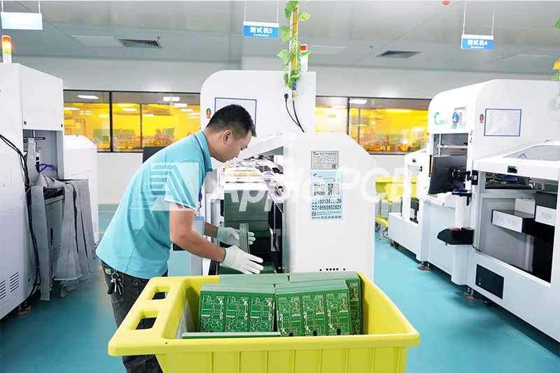
Each small variation like trace width, trace thickness, dielectric constant of the insulating materials, and layer spacing can affect the characteristic impedance of the PCB traces. High speed PCB fabrication is a meticulous process that demands precision and expertise at every stage.
Material Selection
Factors to Select a High-speed PCB Laminate
Selecting a high-speed PCB laminate requires balancing performance and practicality. Consider factors like the target impedance (Dk for higher values, but with practical trace widths), tight Dk tolerance for consistent impedance, low loss tangent (Df) to minimize signal attenuation at high frequencies, and thermal stability (low CTE) to maintain consistent impedance over operating temperatures.
Common High-Speed Laminate Options
Enhanced FR-4 Laminates: Specialized resin formulation improve the standard FR-4 epoxy-glass material and fiber reinforcements, providing enhanced high frequency while maintain a more economical solution.
Rogers Laminates: The Rogers Corporation offers a range of high-performance laminate materials, including the RO4000 series and RO5000 series, which cater to specific requirement in high-speed digital, RF, and microwave applications.
Polyamide Laminates: Polyamide based laminates, such as those from DuPont. These laminates has low dielectric constant and low losses, to make them suitable for high speed digital and RF design.
PTFE (Teflon) Laminate: PTFE laminate features an exceptionally low dielectric constant (around 2.1) and low loss tangent. Therefore, this making them ideal for RF and microwave applications where precise impedance control is paramount.
Ceramic-Filled Laminate: This high performance laminate incorporates ceramic fillers, such as alumina or specialized ceramic compound, to achieve dielectric constant in the range of 3 to 10 along with low loss characteristic. Examples include the Rogers RO3000 series and Taconic TLY series, which are widely used in high-speed digital and RF circuit design.
Hydrocarbon Based Laminate: Laminates made from materials like cyanate ester or polyimide provide low dielectric constants (around 3 to 4) and low losses.
Modified Epoxy Laminates: Laminates manufacturers have developed specialized epoxy resins that incorporate chemical additive. Such as fluorine, to lower the dielectric constant (typically 3.5 to 4.5) while maintaining a more cost-effective alternative to PTFE and ceramic-filled option.
Precise Drilling
Drilling vias (connection points between layers) requires extreme precision to maintain the desired via size and minimize unwanted effect on impedance. Advanced laser drilling technique can achieve better accuracy.
Trace Width and Thickness Variations
Even slight deviations from the designed trace dimensions can significantly impact the final impedance. Advanced electroplating techniques with strict process control ensure consistent trace width and minimize impedance variations.
Surface Roughness
The surface roughness of copper trace can influence the effective trace width and impact impedance. Advanced plating techniques are employed to achieve smooth and consistent surface.
The Difference Between High-Speed PCBs and Impedance Controlled PCBs
In essence, all high-speed PCBs are impedance-controlled PCBs, not all impedance-controlled PCBs are sigh-speed PCBs. While both types of PCBs involve impedance control, the level of precision and the targeted applications differ. Impedance-controlled PCBs are used in a wider range of applications where signal integrity is important, but the operating frequencies might be lower. These PCBs can tolerate slightly looser tolerances in trace dimensions and material properties.
High-speed PCB, on the other hand, are designed for the high-frequency signals. Extremely tight tolerances are required for impedance control.
The Difference Between High-Speed PCBs and High-Frequency PCBs
Although high speed PCB and high-frequency PCB are often used interchangeably there are subtle distinctions between the two.
High speed PCB primarily are crafted to handle digital signals with minimal signal integrity problems, like crosstalk and reflection. They are used in high speed data buses and computer networking equipment necessitating careful consideration like trace impedance, differential pair routing and the use of low-loss dielectric materials.
High frequency PCBs are designed to handle analog signals with minimal loss due to skin effect and dielectric loss, used in RF and microwave application. This requires the use of thicker copper trace and specialized materials.
However today many PCBs require a combination of both high-speed and high-frequency capabilities, making the distinction less clear-cut.
Why Choose ApplePCB?
Rich Experience
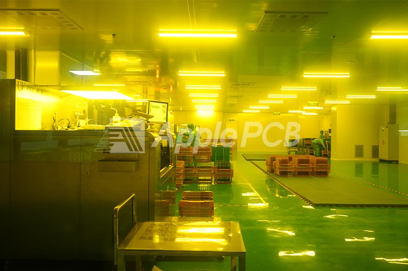
Designing and fabricating high speed circuit board requires specialized expertise that goes beyond standard PCB. As a high speed PCB supplier, ApplePCB deeply understand the unique requirement, performance characteristics, and physical property of high-frequency signal transmission. We have the capability to be your trusted partner for all your high-speed PCB needs.
Raw Material Inspection
We partner with industry leaders like Rogers, Isola, Kingboard and Furukawa Electric source PCB’s laminates, prepregs and copper foils. These advanced materials offer outstanding dielectric properties, low signal loss, and exceptional thermal management - critical attributes for high-speed, high-frequency applications.
Precise LDI Technology
ApplePCB employs LDI (laser direct imaging) technology to eliminate inconsistencies in trace width, further enhancing our ability of high speed PCB production with the consistent impedance, which is necessary to support the high frequency, rapid edge rate, and sensitive signal integrity demand.
