
High speed electronic devices, like smartphones, computers and advanced communication systems need management of impedance to maintain signal integrity and reduce signal loss. With the rising complexity and higher frequencies of these gadgets, the importance of dependable impedance control grows significantly.
Definition of Impedance Controlled PCB
Impedance controlled PCB involves the methods and techniques used to maintain a consistent electrical resistance, along designated signal traces on circuit boards. This ensures reliable signal transmission and minimizes signal reflections and distortions in high-speed electronic devices.
What Is Impedance?
Impedance is a measure of how much a circuit resists the flow of alternating current (AC) at a particular frequency. It's similar to resistance, but resistance is a simpler concept based solely on material properties in direct current (DC) circuits. Impedance considers resistance plus reactive components (capacitance & inductance), making it a complex value (magnitude & phase) that can vary with frequency. Imagine resistance as a simple water pipe and impedance as a complex plumbing system with valves and reservoirs influencing flow behavior.
Applications of Controlled Impedance PCB
High-speed communication devices
● Computer motherboards and graphics cards
● Network routers and switches
● Telecommunication equipment (5G infrastructure)
High-Speed Digital Circuits
● High-speed data transfer ports (USB-C, Thunderbolt)
● High-performance mobile phones and laptops
● Advanced gaming consoles
Embedded systems
● Industrial control systems
● Medical devices
When the PCB Requires Impedance Control?
PCBs require impedance control whenever you're dealing with high-frequency signals generally exceeding 100 MHz in the following situations:
High-Speed Digital Circuits:
For high speed digital signals, such as those found in modern processors, memory, and communication interfaces, mismatched impedances can lead to signal reflections, ringing, and other issues that degrade signal integrity.
High-Frequency Transmission Lines:
High-frequency transmission, like microwave and millimeter-wave circuits, where trace dimensions approach the signal wavelength require a consistent characteristic impedance. At these frequencies, even minor impedance mismatches can cause significant signal reflections, power losses, and other issues that degrade signal integrity.
RF and Microwave Circuits:
In radio frequency (RF) and microwave circuits, strict impedance control is necessary to reduce reflections and optimize power transfer.
Differential Signaling:
Differential signaling, used in technologies like PCIe, LVDS, and USB, requires balanced impedances between the differential pair traces. Impedance mismatches can lead to skew, common-mode noise, and other problems that degrade the differential signal quality.
Analog Signal Paths:
High frequency analog circuits require careful impedance control, such as those involving operational amplifiers, analog-to-digital converters. Impedance mismatches between analog components and PCB traces can lead to reflections, loading effects, and reduced bandwidth, all of which can degrade the fidelity of analog signal.
Power Distribution Networks:
The impedance of the power delivery network, including power planes and vias, can mitigate power integrity issues, like noise, ripple, and transient.
Why is Impedance Control Important?
Signal Integrity
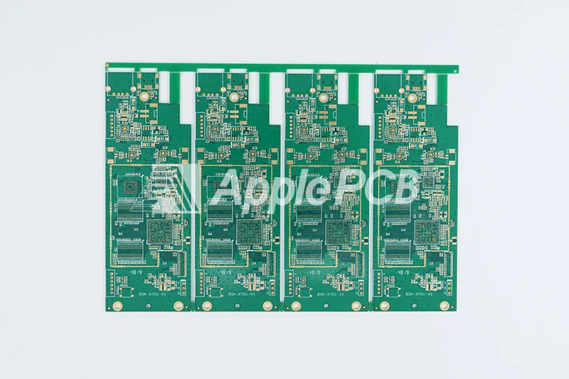
Controlled impedance ensures signals integrity transmitted through the circuit board. By carefully managing impedance, signal distortion, reflection, and attenuation can be prevented. This is vital for applications where data accuracy and reliability are critical such as telecommunications, high-speed data center and medical device.
Reduced Crosstalk
Maintaining controlled impedance is essential for reducing crosstalk, where the signal from one pathway disrupts an neighboring pathway. As crosstalk can negatively impact signal integrity, this is crucial in packed PCBs containing high speed signal pathways.
Prevention of Signal Loss
Signal loss can be an issue, when there are impedance mismatches at high frequency. By using controlled impedance design can reduce signal loss, keep the signal strong and clear.
Lower EMI
Proper impedance control can minimize electromagnetic interference (EMI), helping reduce the emission of unwanted electromagnetic signals, preventing interference with other electronic component and system.
Factors Influencing PCB Impedance
Layer Stackup Design
The arrangement of the layers in a multilayer PCB, known as the stackup, is designed to control impedance. The placement of signal layer and reference ground and power planes is critical. By strategically placing ground planes and power planes around the signal layer can control the distribution of the electric field and achieve the desired impedance.
Dielectric Constant of Material
In most cases, a lower Dk of the core material is advantageous for impedance control and signal integrity. Ideally, the Dk should be consistent throughout the material. Different core materials offer different dielectric constants, which in turn influences impedance, common materials include FR-4 (εr ≈ 4.4) and high-frequency laminates (εr ≈ 3.5 to 3.7).
Trace Geometry
The width and thickness of the copper traces significantly impact impedance. Wider traces generally have lower impedance. By adjusting these dimensions, designers can achieve the desired impedance value for different signal types (single-ended or differential pairs).
Vias
Vias connect traces between layers, can introduce unwanted inductance and capacitance, affecting impedance. Careful via placement and size optimization are crucial for maintaining consistent impedance throughout the trace length.
Routing
Maintaining consistent trace spacing and minimizing sharp turns are key routing strategy to reduce impedance variations.
Types of Traces Structures
Microstrip Line
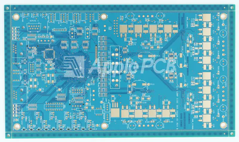
Microstrip is a type of traces structure used in single-layer PCB. In a microstrip configuration, the signal trace is routed on the surface of the PCB. There is a continuous ground plane beneath the microstrip trace, but no ground plane above it. The space above the trace is typically air or the PCB's solder mask material.
Stripline Line
Stripline is a type of trace structure used in multi-layer PCB. The signal trace is sandwiched between two continuous ground planes in a stripline configuration. The ground planes serve to shield and uphold an controlled impedance environment for the signal trace .
Coplanar Waveguide (CPW)
Coplanar Waveguide (CPW) is a traces structure that features a signal trace on a dielectric substrate with a single ground plane on one side and air on the other, offering a compromise between microstrip and stripline configurations. Compared to stripline, while CPW provides similar impedance control and easier to fabricate due to the single ground plane, it is more susceptible to external noise interference.
Methods for Calculating PCB Impedance
Empirical Formula Method
This is a straightforward approach for estimating impedance values in PCB design. Its key advantages are simplicity and speed, making it suitable for rough calculations and initial estimations. However, the accuracy is generally lower compared to electromagnetic field solvers or advanced numerical analysis, and the formulas are only applicable for relatively simple PCB trace geometries.
The most common empirical impedance equations are the microstrip line formula for traces on single-layer boards and stripline formula for traces sandwiched between two ground planes.
Microstrip Line Impedance Formula:

Where:
Zo: Characteristic impedance in ohms (Ω)
h: Distance from the microstrip trace to the reference ground plane (mm)
εr: Dielectric constant of the substrate
W: Trace width (mm)
T = Thickness of the copper trace (mm)
Note: This microstrip line formula is only valid and applicable under the following conditions:0.1 < (W/h) < 2.0, 1 < εr < 15.
Stripline Impedance Formula:
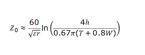
Where:
Zo: Characteristic impedance in ohms (Ω)
εr: Dielectric constant of the substrate
h: Distance between the top and bottom reference ground planes (mm)
W: Trace width (mm)
T = Thickness of the copper trace (mm)
Note: This stripline impedance formula is only valid and applicable under the following conditions: W/h < 0.35, T/h < 0.25.
Simulation Software Method
Simulation software leverages numerical electromagnetic field solvers to deliver precise impedance calculation. Tools like HFSS, ADS, and SIwave can account for a wide range of complex factors in the PCB structure, including vias, copper planes, embedded components, and other impedance discontinuities. The computational capabilities of these simulation tools allow designers to model the entire PCB layout, optimizing trace widths, layer stackups to achieve the target impedance values.
Check ApplePCB’s Capabilities
| Impedance Tolerances | ±5% |
| Layer Count | 1-36L |
| Maximum Copper Thickness | 18oz |
| Minimum Trace Width and Spacing | 2.5mil |
| Minimum Via Size for Laser | 0.1mm |
| Minimum Via Size for Machine | 0.15mm / 6mil |
| Base Material | FR-4, High Tg FR-4, Aluminum, Rogers, etc |
| Board Thickness | 0.2-8mm |
| Thickness Tolerance | ≤1.0mm: +/-0.10mm, |
| >1.0mm:+/-10%. | |
| PCBA Services | SMD, SMT, DIP Component Assembly |
| Surface Finish | LF HASL, plating hard gold, ENIG, ENEPIG, Immersion Tin, Immersion silver, OSP |
| Certifications | ISO9001, ISO14001, CE, RoHS, UL,IATF16949,ISO13485 |
How to Specify PCB Impedance with ApplePCB?
To specify impedance on a PCB, you typically need to consider a few different parameters:
Target Impedance: This is the desired characteristic impedance of the traces, which is often 50 ohms or 75 ohms for common applications.
Trace Width: The width of the copper traces on the PCB directly affects the impedance. Narrower traces generally result in higher impedance .
Trace Height: The thickness or height of the copper traces impacts the impedance. Thicker traces tend to have lower impedance .
Layer Placement: The specific layer or layers on which the impedance-controlled traces are routed.
Spacing: For coplanar or differential trace configurations, the spacing between the copper components, such as the traces and adjacent ground planes, needs to be specified to accurately calculate the impedance .
When dealing with complex impedance needs , it's beneficial to present a comprehensive table or chart that outlines the desired impedance values along with the related trace widths, copper thicknesses and layer thicknesses . Having this aid can assist in effectively conveying the exact PCB impedance requirements and prevent any misunderstanding.
Challenges of Manufacturing Impedance Controlled PCBs
Design Complexity:
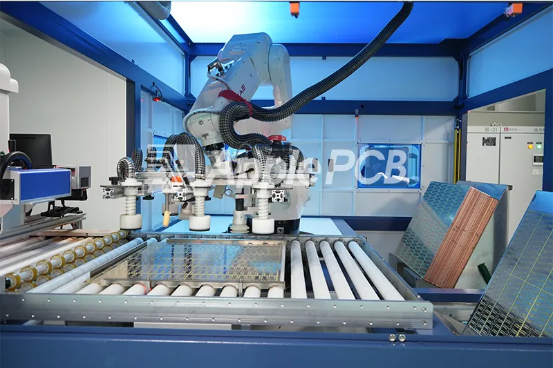
Impedance control PCB requires meticulous design considerations and careful routing of transmission lines to maintain the desired impedance level. Ensuring signal integrity and minimizing crosstalk become crucial.
Material Selection:
ApplePCB offers a variety of laminate materials with well-defined and controlled Dk values. The dielectric constant (Dk) of the substrate material significantly affects the characteristic impedance (Zo) of a trace.
●Lower Dk values generally result in higher impedance.
●Higher Dk values generally result in lower impedance.
Factors for choosing a substrate
Desired Impedance Value: Select a substrate with a Dk that helps achieve the target impedance for your controlled impedance lines.
Dk Tolerance: Opt for materials with tight tolerances on the Dk value to minimize impedance variations.
Thermal Expansion Coefficient: Ensure the Dk value doesn't change significantly with temperature variations, as this can affect impedance over time.
Frequency Range: At higher frequencies, the impact of dielectric loss (represented by the loss tangent) becomes more significant. Choose a laminate with a low loss tangent at your operating frequency to minimize signal attenuation.
Common Laminate Materials for Impedance Control
FR-4: A cost-effective and widely used glass-reinforced epoxy laminate with a Dk range of 3.3 to 4.4. It's suitable for moderate-speed applications with less stringent impedance requirements .
PTFE (Teflon) Laminate : PTFE has an extremely low dielectric constant (εr ≈ 2.1) and low loss tangent, making it suited for high frequency applications. PTFE laminates, such as Rogers RO4000 and Duroid series, provide excellent impedance control and predictable performance up to microwave frequencies.
Ceramic-Filled Laminates: Laminates filled with ceramic particles, like alumina (Al2O3) or specialized ceramic compounds, offer low dielectric constants (εr ≈ 3-10) and low losses. Examples include the Rogers RO3000 series and Taconic TLY series, which are commonly used in RF and microwave circuit .
Hydrocarbon Laminates: Hydrocarbon-based laminates, made from materials like cyanate ester or polyimide, also provide low dielectric constants (εr ≈ 3-4) and low losses. These laminates are suitable for high-speed digital and RF applications where precise impedance control is required .
Modified Epoxy Laminates: Manufacturers develop specialized epoxy resins that incorporate chemical modifications, such as the addition of fluorine atoms, to achieve lower dielectric constants (εr ≈ 3.5-4.5). These modified epoxy laminates offer a more cost-effective alternative to PTFE and ceramic-filled options for high-frequency application.
Fabrication Tolerance:
Trace Width and Thickness: Even minor deviation from the designed trace width and thickness due to etching or plating variations can significantly affect impedance.
Dielectric Constant: Inconsistencies in the dielectric constant of the core material can throw off impedance calculation and lead to unexpected results.
Surface Roughness: Rougher copper surfaces create a slightly wider effective trace width, impacting the final impedance value.
Manufacturing Process Control:
Drilling Accuracy: Irregularities in the fabricated vias, such as inconsistencies in diameter or surface roughness, can introduce undesirable capacitive and inductive effects, impacting the overall impedance .
Plating Uniformity : Uneven copper plating can lead to variations in trace width, impacting the final impedance value.
Process Stability: Maintaining consistent process parameters throughout production is crucial for achieving repeatable impedance values.
Environmental Factors:
Fluctuations in temperature and humidity can impact the dielectric properties of the PCB materials, leading to impedance variations.
Our Technical Support
Meticulous Stack-Up Planning: We meticulously plan your controlled impedance stack-up, ensuring optimal signal transmission characteristics.
Expert Routing Strategies: Our skilled team optimizes routing for both single-ended and differential pair traces reducing signal loss and distortion.
Boosting Signal Integrity : ApplePCB provides advice on positioning of components, vias and coupling capacitors to improve signal integrity.
Precise Length Matching: We excel in adjusting trace lengths for precise propagation delay, contributing to exceptional board reliability .
Advanced Impedance Calculations: We understand the significance of dielectric constant and employ advanced calculations to fine-tune parameters for accurate controlled impedance.
Unwavering Commitment to Precision: With ApplePCB, you can rely on controlled impedance solutions with a tolerance of +/- 5%. This exceptional precision ensures your electronics meet the most stringent signal integrity requirements.
Seamless Application Performance: Our solutions ensure seamless operation of your electronics across diverse applications.
Why Choose ApplePCB?
Extensive Experience
As an impedance control PCB supplier, ApplePCB has extensive experience in manufacturing impedance control PCBs, from meticulously planned controlled impedance stack-ups to optimal routing for both single-ended and differential pair traces, ApplePCB is dedicated to enhancing the performance of your designs.
Skilled Expert
Our engineers are well-versed in the significance of controlled impedance, are ready to help you efficiently design and produce your boards with top notch impedance tolerances.
Precise Process Control
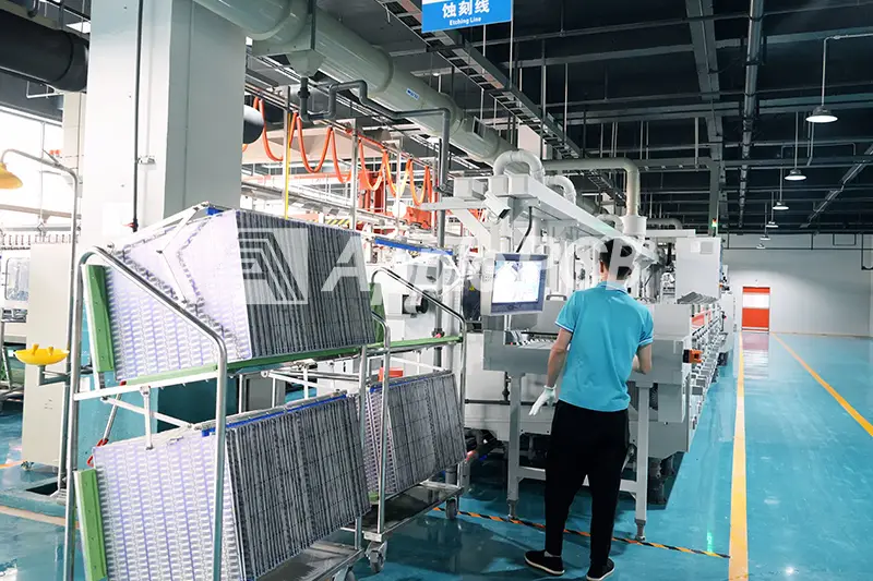
ApplePCB is a professional impedance control PCB factory, has advanced production equipment and a strict quality control system to ensure copper thickness and dielectric thickness, are within the design tolerance. This ensures the final products can achieve precise impedance targets.
State-of-the-Art Facilities
At ApplePCB, we take pride in our state of the art facilities situated strategically in Shenzhen and Chongqing, China. Our Shenzhen plant covers an area of 30,000 sq meters while our Chongqing plant spans 60,000 sq meters. Both locations are fitted with cutting edge Surface Mount Technology and Through Hole Technology machinery to ensure the precise production and assembly of your PCBs.
