Due to the continuous development of the electronics industry, the functions of electronic products have become more complex, so single and double-sided PCB due to crosstalk, stray capacitance and other issues have been unable to meet the demand. Multilayer PCB board was borned. With this article you can learn about multilayer PCB material selection, stackup, and the design and manufacturing process to help you better your project.
What Is Multilayer PCB?
PCBs can be classified based on the number of layers they have such, as single sided, double sided and multilayer PCBs. Multilayer PCBs refer to circuit boards with more than two layers. Multilayer PCBs on the market are usually 4、6、8、10 layer PCB. ApplePCB can produce PCBs with up to 40 layers.
If we liken a circuit board to a road network, then PCB multilayer represents a 3D transportation system. This structure ensures that the layers operate independently from one another while significantly enhancing the efficiency of currents and signals. Hence multilayer PCBs are ideal for compact products.
Nonetheless it's clear that as the number of layers increases the design and manufacturing process, for PCBs become more intricate demanding heightened expertise and manufacturing capabilities from the multilayer PCB supplier.
ApplePCB's Multilayer PCB Manufacturing Capabilities
| Items | Performance parameter |
| Number of Layers | 4-40Layers |
| Material | FR4 Tg 140/150 |
| FR4 High Tg 170/180 | |
| FR4 Halogen-Free | |
| FR4 Halogen-Free & High Tg | |
| Ceramic | |
| PI | |
| Rogers | |
| Metal Core, etc | |
| Board Type | Multilayer Rigid PCB |
| Multilayer Flex PCB | |
| Rigid-Flex Multilayer PCB | |
| Board Size | 600*770mm( 23.62″*30.31″) |
| Board size tolerance | ±0.1mm – ±0.3mm(5%~10%) |
| Board Thickness | 0.4mm – 8mm |
| Board Thickness Tolerance | ±0.1mm – ±10% of thickness of board |
| Min Tracing/Spacing | 3MIL/3MIL |
| Min.Hole Size | 0.1MM |
| Controlled Impedance | 5% |
| Aspect Ratio | 16:1 |
| HDI Capability | From 1N1 to N7N |
| Min Blind/Buried hole size | 0.1mm(4-18 layers) |
| Surface Finishing | ENIG |
| OSP | |
| Lead free HASL | |
| Gold plating (hard gold) | |
| Immersion Silver | |
| Immersion Tin | |
| Plating Tin | |
| Plating Silver | |
| Carbon Ink | |
| Other Techniques | Blind/Buried Via |
| Gold Fingers | |
| Press Fit | |
| Via in Pad | |
| Electrical Test |
Characteristics of Multilayer PCBs
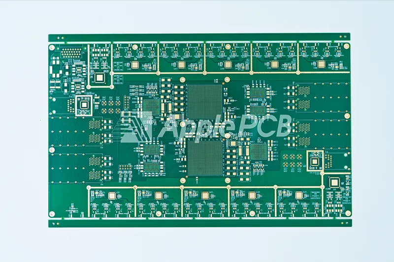
Multilayer circuit boards are usually formed by pressing together multiple layers of prepreg (PP) and core boards. The number of layers is usually even, such as 4 layer PCB, 6 layer PCB, 8 layer PCB, 10 layer PCB, etc. Compared to single- and double-sided boards, multilayer PCBs have a denser circuit arrangement and can accommodate more electrical connections and signal paths. The use of multilayer PCBs allows you to realize very complex electronic circuits on smaller PCBs, significant savings in space and weight.
Besides, multilayer PCB external wiring is reduced to a minimum, electronic components can be installed at higher assembly densities. And effective EMI shielding can be achieved due to the precise positioning of the power and grounding layers. These give them a significant advantage in complex circuit design.
However, this complex design also greatly increases the cost of production and manufacturing, so how to determine the number of layers, in order to meet the performance requirements of the premise of cost savings is very important.
Factors Affecting the Manufacturing Cost of Multilayer PCB
1. Material Cost: the choice of base material will directly affect the cost of multilayer PCB. Generally speaking, the price of high-performance materials such as PI and ceramics will be higher, while the price of FR-4 is more affordable. In addition, the thickness of the copper foil will also have an impact on the cost, 1 oz (35 μm) and 2 oz (70 μm) copper foil cost difference is obvious.
2. Number of Layers: The more layers means the more complex the multilayer PCB production process, the more materials used in the production, and the longer the production time. Because each layer of PCB requires additional lamination, drilling and wiring processes.
3. Production Complexity: Some more complex designs, such as blind and buried holes, smaller line width and spacing require higher precision laser equipment and more stringent quality control, so the cost will be higher.
4. Quantity: Although the higher the number of total price will be higher, but the production of large quantities can dilute some fixed costs (equipment, labor, design costs), so the unit cost will actually be lower than the cost of small quantities.
5. Product Delivery Time: Through cooperation with DHL, FedEx, UPS and other logistics, ApplePCB can provide flexible logistics solutions, including air, sea and land transportation and other ways to meet the delivery time and cost requirements of different customers. If your products need to be delivered quickly, then additional cost may be added, you can refer to our delivery time, if you have specific questions you can contact us in the lower right corner.
| Layer | 2 | 4 | 6 | 8 | 10 |
| The Quickest | 24H | 48H | 48 | 72H | 3 Days |
| Usual time | 4Days | 6-7Days | 7-8Days | 8-10Days | 10-12Days |
| Production | 8-10Days | 10-12Days | 11-13Days | 13-16Days | 13-16Days |
6. Material Supply Chain: The stability of the material supply chain will also have a certain impact on the cost of PCB. In order to ensure the stability of the supply chain, ApplePCB has a long-term reserve of commonly used Laminate in the factory and has established a long-term and stable relationship with a number of high-performance material suppliers (KB, Rogers, Isola, Dupont). Make sure that we can quickly obtain the different materials needed by our customers to avoid any potential supply disruption problems.
7. Geographical Factors: labor costs in different regions have differences; in China and Southeast Asia, PCB manufacturing labor costs are low, while in Europe and the United States are relatively high. ApplePCB operates three facilities. Two are situated in Shenzhen, a leading technology hub, in China, where they focus on creating prototypes and offering manufacturing services for to medium volumes. The third facility is based in Chongqing, an emerging top tier city specializing in high volume multilayer PCB fabrication. This enables us to lower labor expenses while maintaining cutting edge technology and equipment.
If you would like a detailed quote for your multilayer PCB, you can contact us in the lower right corner and we will provide you with a quote within 24h.
ApplePCB's Multilayer PCB Manufacturing Process
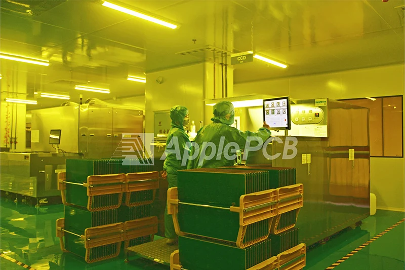
Through advanced equipment and manufacturing techniques, ApplePCB can provide you with reliable multi-layer PCBs, the following is our multilayer PCB manufacturing process:
1. Pre-Production Engineering(PPE)
Based on the gerber files provided by the customer, ApplePCB's team of engineers generates the drawings and drill programs required for production. If there is any problem we will send you an EQ within 24h to ensure the accuracy and consistency of the data. Avoid the risk that unauthorized modification may bring. You can also send us gerber files as soon as possible to speed up your project process.
2. Material Selection and Preparation
Depending on the requirements of the product, we will provide our customers with the appropriate materials from well known brands such as Shengyi, KB, Nelco, Taconic, Panasonic, Rogers, etc. All the materials used can be traced back to their manufacturing batches. We will then cut their selected materials to the required size and keep them in a controlled environment ready for production.
3. Inner Layer Preparation
First we apply a photosensitive layer to the copper-coated substrate on both sides. Then the design pattern is transferred to the photosensitive layer by the latest LDI equipment of Daqo Laser. This process will be carried out in ApplePCB's strictly controlled clean room to ensure the clarity and accuracy of the line graphics. Finally, the unprotected copper foil is removed by chemical etching, and the desired inner layer of the line is formed.
4. Inner AOI
With the advanced Gryphon AOI system, ApplePCB is able to quickly and accurately troubleshoot problems that may occur (open circuits, shorts, leakage erosion, nicks, etc.). Our skilled technicians will assess problematic PCBs to decide if they need fixing or should be discarded. By examining the inspection report engineers will enhance the manufacturing process to lower defect rates and uphold the quality of the end product.
5. Stacking and Lamination
With prepreg and heat we can laminate different inner layers together. I would like to inform you that during this step we strictly control the time, temperature and pressure of the laminator to ensure the quality of the lamination. After the lamination is completed, ApplePCB's specialized technicians will perform quality tests (micro slicing, cross-section thickness verification, peel strength measurements, Hoffman testing, etc.) to ensure the integrity of the lamination and prevent defects such as warpage and delamination.
6. Drilled Hole
ApplePCB's multilayer PCB production lines are equipped with CNC drilling machines and laser drilling equipment. Our CNC drilling machines are perfect for drilling standard and larger sized holes with fast production speeds. However, when extremely small holes need to be machined, we rely on our high-precision Mitsubishi laser drilling machine. This state-of-the-art equipment guarantees extremely high accuracy (±0.01 mm) and can machine holes as small as 0.075 mm.
7. PTH and Panel Plating
ApplePCB's plating process consists of PTH and panel plating. A very thin layer of copper (typically a few microns) is first deposited on the hole walls and the entire panel by a chemical reaction. This step ensures reliable copper plating even on non-metallic hole walls. Next, the thickness of the copper layer on the hole wall is further increased by panel plating on top of the PTH deposits.
The entire plating process requires tight control of current density and plating time to ensure that the thickness of the copper layer is uniform and meets the design requirements. Our standard through-hole plating thickness is 25 microns, which meets IPC Level 3 standards. If you need thicker copper, you can refer to our manufacturing capabilities.
| Finish Copper | Process capability |
| Inner | 18um(1/2oz) |
| 630um ( 18oz) | |
| Outer | 25um(2/3oz) |
| 630um (18oz) |
8. Outer Layer Lines
Similar, to the inner layer circuit, in the layer the outer layer also uses a photographic film to transfer the design pattern through exposure. Subsequently it goes through etching to create the final circuit pattern.
9. Solder Mask
First, we apply liquid or dry film solder masks to the PCB surface. Commonly used methods include spraying, screen printing, or dry film lamination. After curing, the solder mask has good chemical resistance and can effectively protect the copper lines of the PCB to prevent the soldering process of miswelding and short-circuit phenomenon. ApplePCB can provide green, blue, red, yellow, black, and other colors of solder masks to choose from.
10. Screen Printing
Depending on the customer's requirements, we will use advanced text printers to print characters such as component markers, polarity markers, etc. onto the solder mask using screen printing technology. Applepcb utilizes automated screen printing machines that surpass the efficiency and precision of manual screen printing machines ensuring top notch quality, in screen printing outcomes. Selection of durable, chemically resistant screen printing inks can improve the reliability of the characters. If necessary, ApplePCB can provide you with TAIYO (Japan) PSR2000 series, TAMURA (Japan) DSR2200C series and other inks.
11. Surface Treatment
Through automated hot air leveling and chemical plating equipment, we can apply surface treatment to the exposed copper circuits. ApplePCB can provide HASL, LF HASL, ENIG, Immersion Tin/Sliver, Hard Gold, OSP and other surface treatment programs to protect the exposed copper circuits on the boards and enhance the solderability.
12. Final Inspection and Testing
ApplePCB has a comprehensive quality control system with IPC and ROHS quality standard certifications.
First we will rule out open or short circuit problems by flying probe test (small batch) or in-circuit test (large batch). Then the visual quality inspection machine is used to troubleshoot the appearance of multilayer PCBs.
It is worth mentioning that our testing machine and visual quality inspection machine are fully automated without manual handling and intervention. PCB appearance defects can be quickly detected by taking a picture and scanning it, and checking the appearance of a piece of PCB multilayer takes only a few seconds to complete. This makes us more efficient and accurate, with faster delivery time.
Key Process Challenges in Multilayer PCB Manufacturing
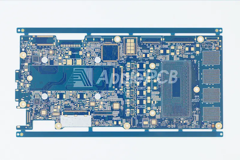
After understanding the manufacturing process of multilayer PCB, we can have a more in-depth understanding of the difficulties that may arise in the manufacturing, if you have other manufacturing questions, you can also contact us in the lower right corner, our professional engineers will provide you with effective solutions.
Internal Circuit Production
If multilayer PCBs use special materials (e.g., high TG, high speed, high frequency, thick copper, and thin dielectric layers), which place higher demands on the production of internal circuits and pattern size control. Impedance control increases the difficulty of manufacturing, and small line width and pitch increase the probability of open and short circuits, affecting the pass rate. More layers of fine lines increase the risk of leakage of the inner layer, and the inner core board is prone to wrinkling and curling, which affects the quality of etching and exposure. In addition, the unit size of multi-layer PCB is larger and the scrap cost is higher.
Interlayer Alignment
Since multilayer PCBs contain multiple layers, interlayer alignment is extremely demanding. Typically, the alignment tolerance of each layer needs to be controlled within 75 microns. Dimensional variations and temperature fluctuations increase the difficulty of aligning multilayer PCBs and complicate precise control.
Pressing Process
The stacking of inner core materials and semi-cured boards is prone to defects such as slippage, delamination, resin voids and air bubble residues. When designing the stacked structure, it is necessary to give full consideration to the material's heat resistance, pressure resistance, adhesive content and dielectric thickness, and other factors to develop a reasonable pressing program. In multi-layer structures, it is difficult to maintain consistent control of expansion and contraction, and thin interlayer insulation can easily lead to failure of interlayer reliability tests.
Drilling
High TG, high speed, high frequency and thick Laminate increase the difficulty of roughness, burr and decontamination during drilling. The increased number of layers leads to increased copper thickness and board thickness as well, which makes drill breakage easy to occur. If the number of BGAs is high, narrower hole wall spacing can lead to CAF failure, and increased board thickness can lead to diagonal drilling problems.
ApplePCB utilizes an advanced drilling machine that automatically swaps out the drill with an one once it hits a specific using frequency. This measure helps prevent drill breakage due, to use ensuring high quality drilling and productivity efficiency, for multilayer PCBs.
Why Choose ApplePCB?
Choose ApplePCB as your multilayer PCB manufacturer and we can deliver:
Cutting-edge Equipments
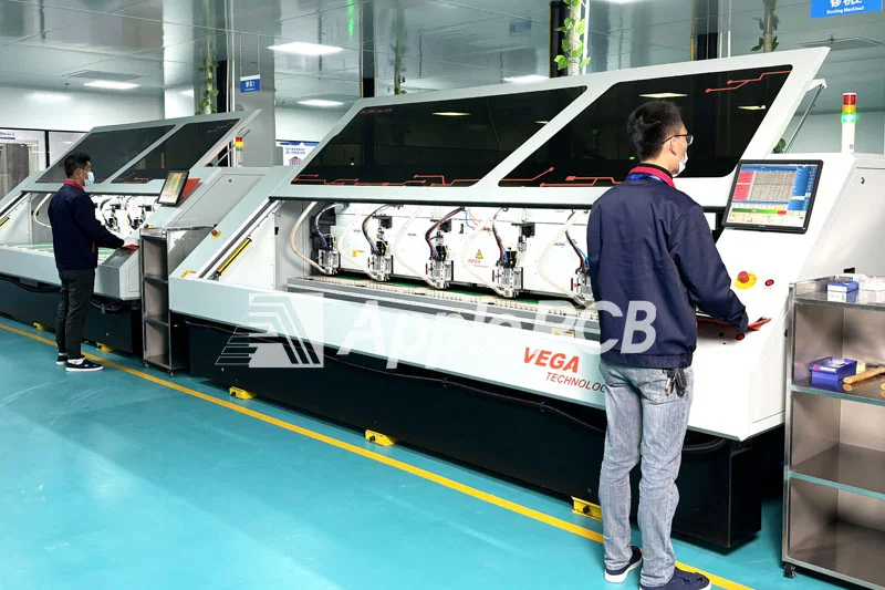
The ApplePCB have cutting edge laminators CNC drilling equipment and laser drilling devices obtained from manufacturers such, as Mitsubishi and Daqo Laser. With over 90% automation the ApplePCB setup guarantees uniformity, in manufacturing and product quality while minimizing issues stemming from human mistakes.
Professional Team of Engineers
ApplePCB has a team of over 100 engineers, each, with, more than 15 years of PCB project expertise equipped to address various intricate multilayer PCB design and manufacturing requirements.
Strict Quality Control
Our quality control system is divided into:
● Incoming inspection
Equipped with staffing 1QC, inspection equipment calipers, micrometers, tape measure, plating measuring instrument, copper foil measuring instrumen.
● Process inspection
Equipped with physical and chemical laboratory and AOI scanning and analyzing machine.
● Function test
Equipped with advanced fully automated function test machine and flying probe machine.
● Appearance testing
Set up a specialized QC team and fully automated appearance testing machine, all products must be inspected according to requirements before shipment.
We also hold several international quality certifications:
●IATF 16949:2024
●ISO 9001:2015
●ISO 13485:2016
●UL
In the meantime, ApplePCB is always committed to environmental protection. We hold the Environmental Management System Certification ISO 14001:2015, ensuring that our manufacturing processes are environmentally friendly and in line with sustainable development.
Considerable Cost Effectiveness
Objective Cost-effectiveness
ApplePCB has its own factory in China, utilizing the local cost advantage and complete supply chain system, we can provide you with considerable cost-effectiveness, so that you can obtain reliable multi-layer PCBs within a limited budget. You can contact us in the lower right corner, we will provide you with a quotation within 24h.
