
When it comes to creating electronic devices designing printed circuit boards plays a crucial role that cannot be understated. Every stage in the PCB design process significantly influences the following manufacturing and assembly steps, determines the reliability of the end product. In this article, we will show you the main steps in designing a PCB, the key point of different types of PCB design, and how we can help you with your PCB design.
How to Approach PCB Design?
ApplePCB as a PCB specialist with 15 years of experience, can provide one-stop service for PCB design, manufacturing, assembly, and component selection. We has outlined 7 steps, for circuit board design to facilitate a progression of your project from desgin to manufacturing.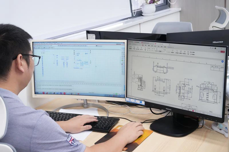
First Step: Defining Key Electrical Parameters for PCB Design
Early in the design process, we need to determine the maximum expected current of the PCB and the operating voltage of the system to ensure that the rated current capability of the alignment and component is sufficient to prevent overheating or damage. Next, it is important to identify whether the signal type is digital, analog, or mixed, and to control the impedance of the alignment according to the need for high speed or high frequency signal, thus improving signal integrity and reducing reflection and noise. In addition, shielding strategy are developed based on EMC.
These are just some of the key point in design, but of course there are many other factors to consider. If you need more indepth professional advice, you can always contact ApplePCB's professional engineer for a consultation.
Second Step: Designing the Schematic
Whether you're using a template or starting from scratch, the first step in creating a printed circuit board (PCB) is designing the schematic, it serves as the foundation for the entire design. It essentially representing the electrical design for the PCB's purpose and functionality. The schematic details which components are used—such as resistors, capacitors, inductors, connectors, and integrated circuits (ICs)—and how they are interconnected.
For PCBs with more complex designs, hierarchical schematics can map out how components relate across multiple levels of design. In short, the schematic provides a clear and organized way to define and modify circuit connections, making it easier to manage the design structure. Moreover, as circuit network become more intricate, adding annotations to the schematic is crucial. Clear and descriptive net names help you track component connection, making placement and routing more efficient.
Third Step: Capturing the Schematic
If the schematic serves as the project's blueprint, then schematic capture is the process of turning that blueprint into a detailed construction plan. This step is not only does it ensure accurate and functional electrical connections, but it also makes the design easy for team members to understand while offering clear guidance for manufacturers. ApplePCB advise considering the following key points during schematic capture:
1. Ensure Consistent Logical Flow
When organizing component symbol and connecting network in the schematic, it's vital to maintain consistent logical flow and connectivity. This is particularly vital for high-speed circuits, as the PCB layout later relies heavily on how signal paths are arranged in the schematic.
2. Strategic Symbol Placement
When placing symbol, make sure there's enough space to keep network connections clear and readable. This prevent confusion over pin numbers and network names, setting the stage for a smooth design process.
3. Flexible Adjustments
Don't stick rigidly to the initial placement of symbols and networks—adjust them as needed for better organization. With robust schematic capture tools (like Mentor PADS®, Allegro, or Altium), you can easily move symbols and tweak circuit regions without worrying about overlapping reference designators, part numbers, or text.
4. Define Rules and Constraints Early
While most design rules don't kick in until the PCB layout phase, defining categories for networks and components during schematic capture helps the layout stage to refers specific constraints, ensuring the final design aligns with project requirements.
5. Include Essential Information
Beyond circuit connection, your schematic should include key project details like product numbers, revision levels, contact info, and copyright data. This information is important for later stage like manufacturing and maintenance. At ApplePCB, we will ensure this information is accurate.
6. Conduct Design Rule Checks (DRC)
Running a DRC during schematic design is vital for catching issues like missing pin connections. ApplePCB rigorously enforces DRC protocols, ensuring the schematic is error-free before moving on to layout, ultimately delivering reliable designs to our clients.
Fourth Step: Establishing PCB Layout
After a series of preparatory steps, we finally arrive at the stage of establishing the PCB layout, where all designs are transformed into reality. Just as workers follow a construction plan to build a house, ensuring that every brick and beam is placed correctly, this step in PCB design physically realizing the design ready for production. Several key steps require special attention to ensure that the design data is accurate and smoothly transitioned into a functional physical board.
1. Update and Confirm Component Footprints
Double check that every component in the schematic has the correct PCB footprint, ensuring this data imports smoothly into the layout database. For custom symbols or components from external libraries, it's critical to confirm that the symbols align with the intended footprints.
2. Generate and Import the Netlist
The next step involves generating the netlist, which contains key information like component designators, footprints, pin connections, and design rules. Although different design tools may handle netlist generation differently, the goal is to convert schematic data into the electrical connections needed for layout.If a layout database hasn't been created yet, this is the point to define the board outline, layer stack-up, required footprint data, and other design parameters (like vias). Once ready, import the netlist into the layout database, ensuring that the electrical connections defined in the schematic are properly implemented in the layout.
ApplePCB offers full technical support during this process, from generating precise netlists to seamlessly importing them into the layout database, guaranteeing accurate data handoff at every stage.
3. Identify and Resolve Potential Issues
Even after extensive check of the schematic and netlist, unexpected issues can emerge after importing into the layout tool, like mismatched pin count or footprint discrepancy. To minimize errors and warnings during layout, ApplePCB typically prevents and resolves potential problems by setting up instructions and design rules at the schematic design stage. For example, in Altium Designer, you can use the Error reporting tab to see all errors. You can also set up the “Directives > Generic No ERC” directive if you want to ignore specific electrical rule checks.
4. Component Placement
With potential issues resolved, you can move on to placing components. Start by positioning component footprints within the PCB's defined outline. During this step, network connections appear as ‘ghost-line', giving a clear view of how components are connected. For optimal performance, strategic component placement is key—considering factors like connectivity, thermal management, electrical noise, and physical constraints such as connectors and mounting hardware. It's also essential to consider manufacturability, ensuring that component locations are suitable for mass production and assembly.
5.Routing Design
Once the components are placed, the PCB routing can begin. This step involves translating the network connections into actual traces, along with the design of power and ground layers. During routing, designers must carefully control the length of the traces to suit the signals they carry, while avoiding signal paths through high-noise areas. This prevents issue like crosstalk and signal integrity problems, preserving the performance of the PCB.
6.Power and Ground Layer Design
Active components like ICs and related parts need reliable connections to power and ground networks, typically achieved through solid plane layers. However, designing power and ground planes is more intricate than it seems. These layers not only distribute power but also provide return paths for signals. Excessive holes, cuts, or gaps in these planes can introduce noise, degrading overall board performance.
Fifth Step: Final Rule Check
The design enters its final phase, the final design rule check and adding text and markings for silkscreening on the outer layers, which help identify components, board details, and copyright information. Next, you'll need to generate manufacturing and assembly drawings. Tools from ApplePCB can provide cost estimates for board production, ensuring you're well-prepared for the manufacturing process.
Sixth Step: Working with PCB Manufacturer
Once your Gerber file is ready, send it to your PCB manufacturer to kick off the production process, which involve fabricating the bare board, assembling component, and performing final test. Choosing ApplePCB's one-stop service to streamline your project. By handling everything from design to manufacturing, from assembly to testing on a single platform, ApplePCB minimize your time and costs involved in dealing with multiple suppliers, reduces communication errors, and ensures consistent product quality throughout the process.
Various PCB Design Services
For different types of PCBs, the key points we need to pay attention to vary. Drawing on 15 years of experience in PCB design and manufacturing, ApplePCB has compiled a list of considerations for different types of PCB designs.
1. Flex and Rigid-Flex PCB Design
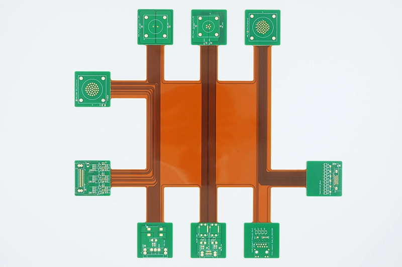
● Routing in Flexible Area: When designing trace in flexible regions, it's crucial to select appropriate bending angles, using curves instead of sharp corners to minimize stress.
● Pad Design: For single sided bend, a rounded pad design with "rabbit ears" (anchoring spurs) is recommended. This design allows the cover layer to capture part of the pad shape, enhancing the overall durability of rigid-flex pcb.
● Static Bend Ratio: Establish the ratio of bend radius to circuit thickness. For multilayer circuit, aim for a bend ratio of at least 15:1; for double-sided circuits, the minimum should be 10:1; and for single-layer circuits, it should be 5:1. In dynamic applications, the bend ratio should ideally be between 20:1 and 40:1.
● Material Selection: In flexible areas, opt for rolled copper due to its superior ductility compared to electrolytic copper.
2. Heavy copper PCB Design
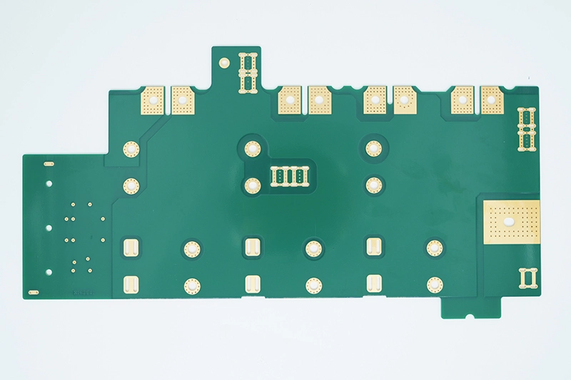
● Choosing the Right Copper Thickness: In heavy copper PCB design, selecting the appropriate copper thickness is vital, it usually ranging from 105μm to 700μm. Accurate calculations of current density and required copper thickness during the design phase are vital to ensure that the board can handle high currents without leading to overheating.ApplePCB can also provide subsequent production services for your heavy copper PCB designs.
● Optimize trace: To enhance the performance of heavy copper PCB and prevent short circuits caused by high currents opt for wider traces and increased spacing between them. Be cautious not to extend the traces as it may result in signal loss and unwanted noise interference.
● Effective Thermal Management: Proper thermal management require consideration of current distribution and heat dissipation paths. Adding copper layers or using special heat sink vias during design can significantly improve heat dissipation.
3. HDI PCB Design
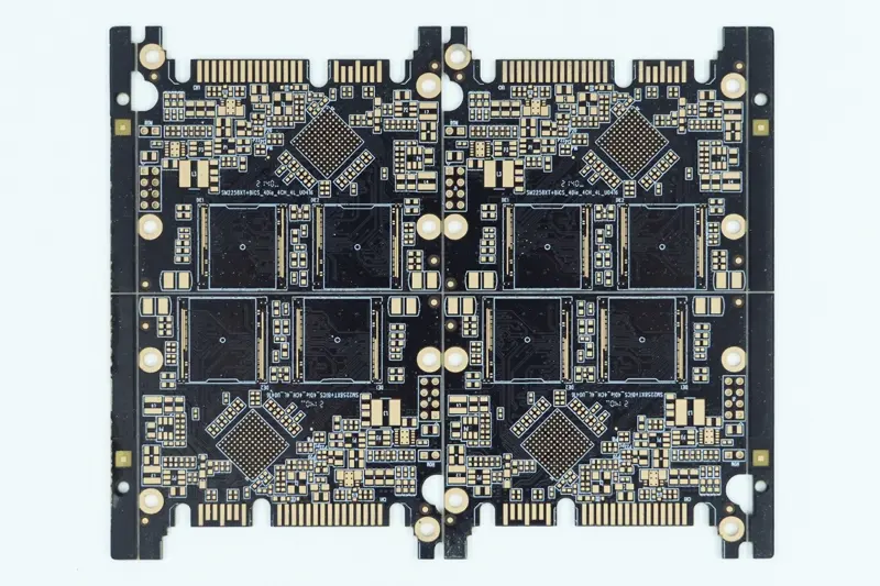
● Microvia and Buried Via Design: Designing HDI PCBs relies significantly on micro blind vias and buried vias to achieve high density interconnections. It is vital to design and position these microvias to ensure signal transmission.
● Managing Hotspot: During the design phase, it's crucial to identify potential hotspot and address them by incorporating through holes, thermal management component, and optimizing the spacing of component to mitigate heat issue.
● Design for Manufacturability (DFM): HDI PCB design require strict adherence to DFM guideline. This includes considering limitations on trace width and spacing, annular rings and aspect ratios, impedance control within the layer stack-up, and the necessary impedance profiles for the stack-up or layer pairs.
4.High Speed PCB Design
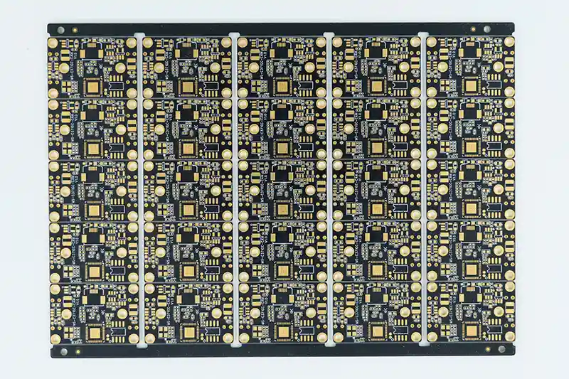
● Via Design: In low frequency circuits, via have minimal impact, but in high speed circuits, they can cause discontinuities in capacitance and inductance, leading to signal impedance mismatch and reflection issue. ApplePCB address these challenges by optimizing via design, which includes reducing the annular ring size, increasing the gap between vias and adjacent planes, removing via stubs through back-drilling, or using microvia. These strategies help minimize the negative effects of via on signal quality.
● Crosstalk Mitigation:Crosstalk Mitigation: Crosstalk is a major concern in high-speed signal design as it can compromise signal integrity. Key strategies to reduce crosstalk include impedance matching and designing effective signal return paths. Additionally, employing the ‘’3W rule,’’which maintains a distance between potential aggressor and victim signals of at least three times the trace width, can further mitigate crosstalk.
● Signal Timing and Synchronization: Signals typically operate in sync with others, such as when transmitting a byte of data, where not only must the byte arrive on time, but each bit must also arrive simultaneously. This transmission duration and the differences in bit arrival times, are influenced by factors like trace length and transmission medium. Effective management of these factors requires careful attention to component placement, material selection, and the matching of trace lengths during the design process.
5. High-Frequency PCB Design
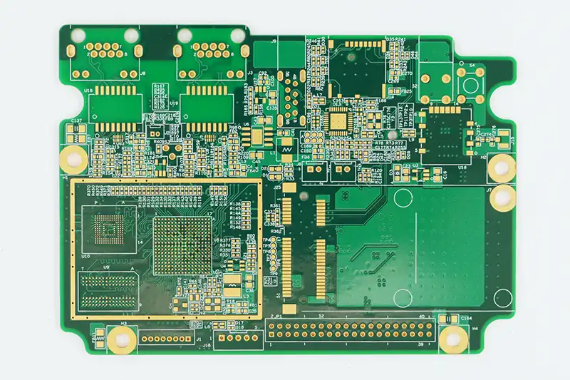
● Minimizing Via Usage: In high frequency circuit design, it's important to limit the number of via, as each via introduces about 0.5pF of parasitic capacitance. By reducing via usage, you can enhance signal transmission speed and lower the chances of data errors.
● Optimized Routing: When routing high frequency signal, use curved traces instead of sharp angles. If angled turns are necessary, 45° angle is recommended as it help minimize signal reflection and loss.
● Stack-up Considerations: In high-frequency PCB stack-up design, it's vital to separate digital and analog grounds due to their significant voltage differences. Additionally, applying the 20H rule to the power layer can reduce plane coupling, allowing any edge-coupled signals to be absorbed by the ground plane. This improves the circuit's electromagnetic compatibility by preventing unwanted radiation.
How Can ApplePCB Help With Your PCB?
At ApplePCB we offer a full range of services, whether you are starting from scratch and need help with design from our team of professional or you already have preliminary PCB design drawing and would like us to assist with production and assembly.
1. What Is Your Idea?
We will first talk to you to find out what function you want this board to fulfill. What equipment or environment will the PCB be used in? Are there any special temperature, humidity, or immunity requirement? Do you have certain requirements for board size, number of layer, material selection, and electrical capabilities? As well as any other specific requirements. To clarify your design needs and PCB project objectives.
2. Is There Basic Files?
As we mentioned earlier, you need to prepare the schematic, package library, bill of materials (BOM) and other basic information before PCB design. If you have already prepared them, you can send them to us to help us design more accurately. If you are just starting your design and haven't completed these preliminary information, don't worry, ApplePCB's team of professional engineers can support you throughout the whole process, creating schematic diagrams for you from scratch and customizing the right package library according to your needs.
3. How Do We Design?
During the design phase, our engineers will utilize various advanced design software (such as Altium Designer, Cadence Allegro, KiCad, etc.) to design the layout of the circuit board according to your need, including the placement of components, the route of the wiring, and so on. After the PCB design is completed, we will convert the circuit diagram into a standard gerber file and confirm all the detail with you. As soon as you give us your nod of approval, we can send them to production!
4. How Do We Ensure the Reliability of the Design?
● Design Rule Check (DRC): Types of check include geometry, gap, alignment width, drilling, and electrical check. In addition to the standard DRC, we can also perform customized checks based on specific project requirements such as high frequency, special stack up, and high power to ensure that any needs not covered by the standard DRC are also met.
● Design for Testability (DFT): To ensure that every board can be easily tested, we incorporate DBG, PROG connector, integrated test point, built-in self-test (BIST), and boundary-scan into our circuit board design. These design element make it easier for boards to detect faults and even self-test after production. This greatly reduces the time and cost of rework and repair.
● Design for Manufacturability (DFM): The goal of DFM is to optimize a PCB design so that it is easier to manufacture and process in real-world production, resulting in lower production costs, higher yield, and fewer potential problem. For complex PCB designs, DFM analysis may be performed more than once. DMF analysis is required when selecting components when performing floorplanning, when placing components, and when planning stackup to identify potential problem as early as possible.
● Design for Assemblability (DFA): Again, we optimize the PCB design, but DFA focuses more on making the PCB smoother and more efficient in the assembly process. First, we will optimize the board layout to determine the spacing between component, soldering direction, and way to reduce assembly costs. Next, the Gerber or ODB++ files are verified to ensure that the gaps and directions of the component traces meet the design standards; finally, the specific requirements for wave soldering, reflow soldering and manual soldering are clarified to ensure the efficiency and reliability of the entire assembly process.
ApplePCB’s Design Services
| Layer Count | 1-34L |
| Build Time | 1 Day –5 weeks |
| Order Quantity | 1–50,000 pcs |
| Material | FR4, PI, Aluminum, Ceramic, PTFE, etc. |
| Maximum BGA | 100+ |
| Maximum Connections | 78000+ |
| Maximum Speed Signal | 122G-PAM4 |
| Board Type | Rigid PCB Flexible PCB Rigid-flex PCB HDI PCB Heavy Copper PCB High TG PCB Multilayer PCB Gold Finger PCB Halogen Free PCBs Impedance Controlled PCB High speed PCB High Frequency PCB Aluminum PCB Ceramic PCB |
| Quality | Standard IPC Class 1/2 |
During the PCB design process, customized design demand special attention and meticulous detail. Whether you're developing a custom PCB or seeking PCB services—from design to manufacturing—ApplePCB is here to assist. We understand the complexities and challenges involved in custom PCB design, and our experienced team is equipped to handle even the most intricate design requirement. If you have any PCB board design need, don't hesitate to reach out to us in the bottom right corner.
