In today’s electronic design, how you structure your PCB layer stack up significantly impacts circuit capability, signal integrity, and overall product reliability. As electronic devices grow more complex, carefully planning your PCB stack-up is not only for minimizing electromagnetic interference (EMI) but also for improving electrical properties and optimizing cost, facilitating a seamless shift to manufacturing. This article will explore the materials, layer configurations, types, and design guidelines for PCB layer stack up, helping you achieve an efficient and dependable PCB stack up design.
Understanding PCB Stack Up Basics
The PCB layer stack-up describes how signal, power, and ground layers are arranged in a printed circuit board. Typically, a PCB consist of alternating conductive copper layers and insulating layers. Signal layer carry electrical signals, while power and ground layers provide stable references for power distribution. Insulating layer prevent electrical shorts by separating the conductive layers. While FR-4 is commonly used for insulation, other materials can be selected based on specific application needs.
Flex PCB Stackup
Flexible PCB generally use polyimide as the substrate, with copper layers and a protective coverlay. A standard flexible PCB stackup usually include 1 to 2 copper layers, laminated together to create a structure. Additional stiffeners can be incorporated to enhance rigidity based on design need. The main benefit of flexible PCBs is their ability to bend and move freely while maintaining electrical integrity, making them well-suited for dynamic use cases.
Rigid-Flex PCB Stackup
Rigid-flex PCB offer a blend of the mechanical durability found in rigid boards with the flexibility of flexible circuits. In such stack-ups, flexible layers are usually sandwiched within rigid layers, creating a unified board with both rigid and flexible sections. The flexible regions can bridge multiple rigid sections, achieve signal and power transmission while retaining flexibility. To improve performance in these flexible zone, cross-hatched copper layer are often utilized instead of solid copper, enhancing flexibility while still ensuring effective shielding.
HDI PCB Stackup
HDI PCB stack up designs are known for their compact structure and high-density packaging, making them ideal for applications requiring high-performance processing and high-speed signal transmission. These PCBs typically feature blind, buried, and microvias, enabling accommodating intricate routing needs through dense interconnections. Manufacturing HDI PCBs often involves 1+N+1 or 2+N+2 configurations, with multiple stackup where each layer requires precise microvia alignment and high-accuracy processing. Proper microvia filling and handling are crucial since they directly affect interlayer electrical connections and signal performance. ApplePCB ensures the reliability of HDI stack-ups through precision microvia processing, signal integrity management, quality checks, and adaptable solutions for complex designs such as BGA.
High Frequency PCB Stackup
High-frequency PCB stack-up are engineered for application requiring fast signal transmission and high-frequency ranges, sometimes reaching up to 100 GHz. Commonly used in RF and microwave fields like communication systems, satellite technology, and radar, these boards require careful material selection. Using low Dk and low Df materials is essential to minimize signal distortion and loss. ApplePCB is proficient in working with high-frequency materials such as Rogers, and our precision manufacturing equipments and technology ensure consistent impedance and tight tolerance control.
Best Practices for Prepreg Selection and Interlayer Alignment
Prepreg refers to a resin-infused reinforcement fabric used for bonding layers in PCB manufacturing. Each type of prepreg, characterized by distinct properties like thickness, strength, and resin flow, play a role in the final board capability. ApplePCB supplies options like 7628, 2116, and 1080, tailored to meet varying design needs.
| Type | 7628 | 2116 | 1080 |
| Resin Content (%) | 48.0 ± 3.0 | 53.0 ± 3.0 | 64.0 ± 3.0 |
| Resin Flow (%) | 30.0 ± 5.0 | 31.0 ± 5.0 | 41.0 ± 5.0 |
| Gelation Time (s) | 100 ± 20 | 105 ± 20 | 105 ± 20 |
| Thickness (mm) | 0.18 | 0.1 | 0.06 |
| Thickness after Solidification (mm) | 0.23 ± 0.02 | 0.13 ± 0.03 | 0.09 ± 0.01 |
Prepreg thickness isn’t standardized, it’s adjusted based on design requirements to achieve the desired PCB thickness. Deciding on the number of prepreg layers involves considering inner layer thickness, overall design thickness targets, manufacturing constraints, and specific properties and test data of the prepreg. In addition, ApplePCB recommends the following precautions for stack-up measling and interlayer offset, which can easily occur during the stacked.
● Interlayer offset: In PCB design, incorporating resin grooves at the edges can replace traditional dam pads. For accurate layer alignment, using hot-melt rivets and alignment pins is recommended to minimize interlayer offset and ensure precise stack-up.
● Stack-up measling: Introducing silicone pad in combination with epoxy boards during the board arrangement process helps balance pressure. This approach not only prevent measling in the stack-up but also maintains consistent board thickness.
Standard PCB Stack-up with Different Layers
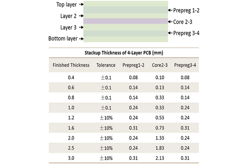
One of the common choices is 4 layer stack up. For more complex tasks you might consider using a stack with six, eight ten or even twelve layers.
4 Layer PCB Stack Up

1. Signal-Ground-Power-Signal
This is a standard 4 layer PCB stack up configuration. The ground and power layers are positioned between the signal layers, effectively balancing power and signal need. This setup offer a low-impedance return path, which reduces noise and crosstalk, making it suitable for most applications. However, it may have some limitations when handling high-speed signals.
2. Signal-Power-Ground-Signal
In this layer arrangement the power layer is placed close to the top signal layer with the ground layer positioned near the bottom signal layer. This setup enhances signal transmission. Maintains power integrity by keeping the power layer in proximity to the signal layer. It works well for high power devices as it reduces voltage drop and ensures a power source. However this configuration could lead to noise levels in the signal layer compared to the initial stack up.
3. Ground-Signal-Signal-Ground
The configuration involves having two signal layers sandwiched between two ground layers establishing a continuous grounding path that ensures low-impedance current return and minimizes signal interference. The stack up supports stripline routing, which effectively reduces crosstalk and enhances signal integrity. Although this four-layer stack-up is complex and costly to produce, it is typically used in RF and communication equipment where where minimizing EMI and ensuring signal performance are vital considerations.
4. Signal-Ground-Ground-Power
This stack-up includes dual ground layers, which is uncommon. The design improves shielding and noise reduction, resulting in better signal integrity. With a dedicated power layer, it’s well-suited for high-power applications. As a result, this configuration is often chosen for analog circuit and mixed-signal device that demand superior noise suppression and efficient power distribution.
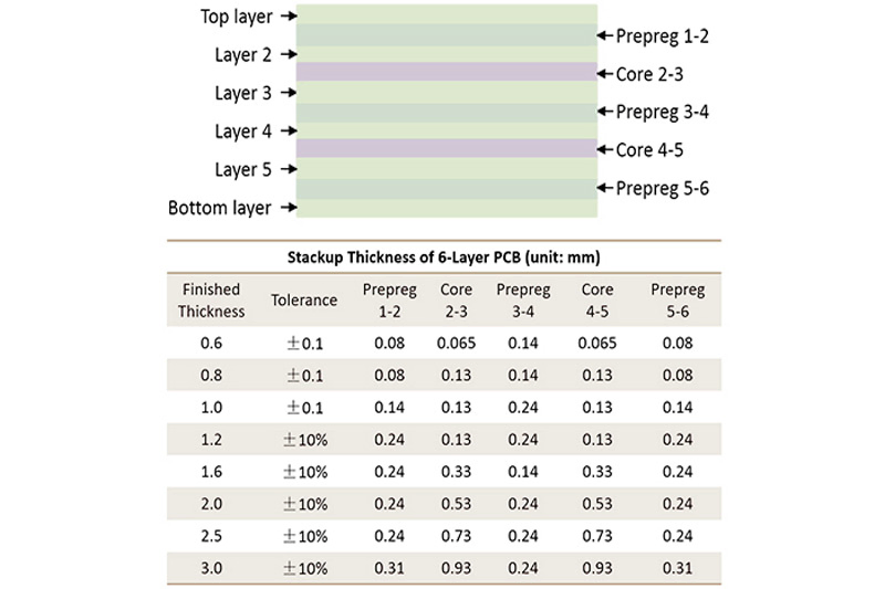
6 Layer PCB Stack Up

When balancing cost and performance is essential, a 6 layer stack-up is often a good option. The standard configuration for a 6 layer PCB include a top signal layer, ground layer, inner signal layer, power layer, ground layer, and bottom signal layer. By adding extra ground and power layer, this design offer improved EMI control, enhanced signal integrity, and better ESD protection.
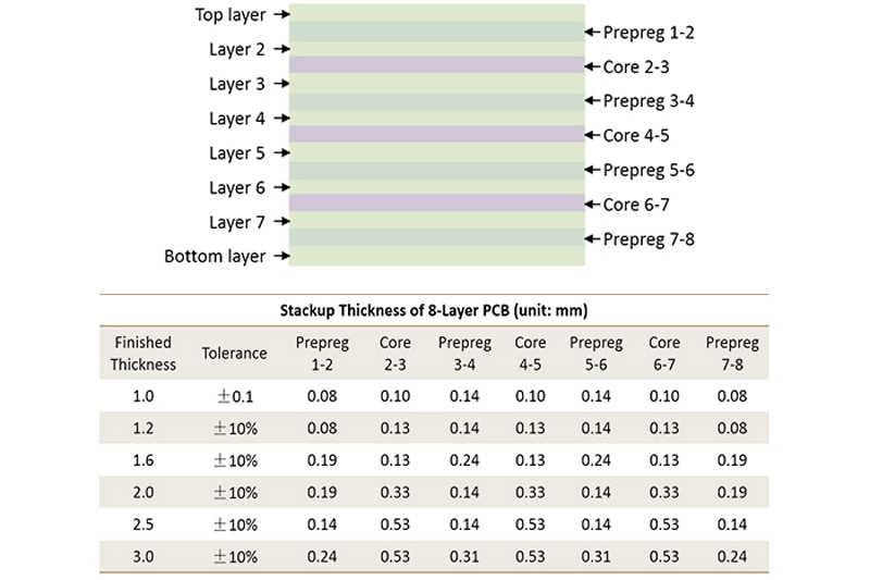
8 Layer PCB Stack Up

The signal layer of the 8 layer PCB stack up is separated by the power and ground planes, and additional power and ground planes are added. This stacking helps reduce crosstalk between signals and improves signal integrity. However, due to their complexity, 8 layer stack up are more complicated and costly to design.
PCB Layer Stack-Up Guidelines
Creating a dependable and effective PCB stack up design involve adhering to steps and optimization strategies. In the discussion we will delve into these steps extensively to assist you in attaining the best design results.
1. Specify Electrical and Mechanical Needs
● Board Type: Decide on the type of PCB needed whether its HDI or High Speed, Rigid or Flex PCB. Each type of PCB stack comes with its set of design consideration.
● Number of Signal and Power Layers: Determine the number of PCB layers based on the application requirement to meet both signal integrity and power distribution need.
● Material Requirements: Choose laminate materials and copper layer thicknesses that align with the design specifications to ensure the PCB electrical capabilities and mechanical resilience.
2. Impedance Control and Routing Design
● High-Speed Traces: Focus on minimizing interference when designing high-speed signal paths, and optimize routing to reduce crosstalk effectively.
● Power Distribution Network (PDN): Structure the power and ground layers to maintain low impedance paths and ensure stable power delivery throughout the design.
● Layer Allocation and Via Trace Width: Carefully plan inter-layer routing and via sizes to maintain controlled impedance and uphold signal integrity across the PCB.
3. Design Validation and Optimization
● Signal Considerations: During the design stages, perform analysis for RF, analog, and digital signals to tune overall circuit performance.
● Blind and Buried Via Considerations: Evaluate whether the use of blind or buried vias is necessary based on manufacturing complexity and signal transmission requirements.
● Board Dimensions and Hole Tolerance Checks: Confirm that the PCB’s dimensions and hole tolerances meet manufacturing specifications and quality standards.
● Class 2 and Class 3 Compliance: Assess the design to ensure it aligns with Class 2 or Class 3 standards, depending on the required reliability level.
4. Partner with the Manufacturer
The primary aim of the design is to produce a PCB that meets the intended specifications. It's an idea to communicate with your PCB manufacturer in the stages to verify their production capabilities and ensure that your PCB stack up design can be smoothly transformed into a product ready for manufacturing. You can also leave a message in the bottom right corner of this page and share your gerber file with us. Our engineering team will conduct a DFM analysis to help ensure your design transition smoothly into production.
5 Tips for Designing an Effective PCB Stack-Up
Once you’ve carefully considered the upper key factors in the initial design phase you can proceed to the more intricate design phase. Here are 5 helpful tips to help you design the effective PCB stack-up.
1. Material Selection
Opt for materials with superior electrical performance that also align with assembly needs. When choosing substrate materials, focus on their dissipation factor (Df) and dielectric constant (Dk) to reduce signal distortion and loss. For copper layers, the current carrying capacity is critical—higher currents demand thicker copper layers to maintain circuit stability and reliability.
2. Determine the Optimal Layer Count
The number of signal layers plays a critical role in PCB performance. Applications involving high-speed or high-power circuits often require more signal layers to accommodate complex designs. For components like BGAs with high pin counts and tight spacing, additional layers are necessary for effective routing. Strategically assigning ground and power layers not only optimizes signal layer layout but also ensures ideal return paths for high-frequency and time-varying signals, reducing noise, crosstalk, and EMI. This approach enhances both signal integrity and electromagnetic compatibility (EMC).
3. Trace Routing and Impedance Control
In PCB stack-up design, accurate trace routing and impedance control are crucial for maintaining signal integrity. High-speed signals are best routed within internal layers sandwiched between ground planes to mitigate crosstalk and EMI. Placing signal layers adjacent to reference planes helps maintain consistent impedance and effective shielding, which in turn reduces EMI and enhances signal quality. This approach also limits trace loop radiation and lowers electromagnetic emissions, ensuring reliable circuit performance.
4. Thermal Management
Proper thermal management is a crucial aspect of stack up design. Effective heat control prevents overheating, ensuring that electronic devices function at peak performance. This requires strategic use of heatsink, thermal via, and optimized component placement. By incorporating thermal via in key areas, heat can be efficiently dissipated, reducing the risk of overheating. Positioning high-power components near heatsink accelerates heat removal, extending the lifespan of components and enhancing the system’s overall efficiency.
5. Via Types and Placement
In a PCB layer stack up, vias are essential for connecting different layers, and their placement and type are critical to signal transmission. The most common via types include buried vias, blind vias, and through-holes. While blind and buried vias are more complex to design and manufacture, they are excellent for saving space and minimizing interference. Through-holes are stable but can complicate routing in multilayer boards. To maintain the best signal integrity, careful via placement is essential. ApplePCB specializes in buried, blind, and through-hole technologies and uses techniques like stitching, back-drilling, and laser drilling to tune impedance, reduce crosstalk, and enhance signal quality.
Conclusion
In this evolving technology field, ApplePCB, with its over 15 years experience and advanced technical advantage, is able to help customer cope with complex stacked designs ranging from 4 to 12 layers and even higher counts. Whether it's high-speed signals, dense packages, or special process requirements, we are able to provide accurate and efficient solutions. If you need customized multi-layer PCB manufacturing support, please feel free to contact us.
