When designing printed circuit boards (PCBs), the silkscreen layer might not be the first thing that comes to mind, because silkscreen is not always a mandatory step in PCB manufacturing, its inclusion can significantly enhance the usability and professionalism of the product. Silkscreening provides important information for assembly, troubleshooting, and user interaction. In this guide, we will explore the definition of PCB silkscreen, effective design tip, the manufacturing process, and how to select the right type of silkscreening for your project.
What Is Silkscreen in PCB?
In pcb design the silkscreen refer to a layer of text or pattern printed by ink on the surface of a PCB. The material used for silkscreen printing are usually non-conductive epoxy ink that have been specially formulated to make these resin heat and chemical resistant for soldering and assembly.
Silkscreen character are like a clear map for manufacturer and engineer who need to test, repair or assemble circuit boards, helping them to quickly find the location of each component, reducing the chance of error and improving work efficiency. Of course, not all circuit boards need to be silk-screened because it will add some extra costs, so we usually only add silk-screening when the customer explicitly requests it.
What Are the PCB Silkscreen Symbols?
If the size of the board is limited, then we can prioritize the printing of key information and discard some unnecessary characters as required. As for the content of pcb silkscreen symbols, it usually includes:
| Type | Content |
| Test Point | Identifies the location of the test point to facilitate measurements and troubleshooting. |
| Warning Flags | Specify higher current, power, and voltage values. |
| Reference Flags | Indicate values for resistors, inductors, and other components to prevent components from preventing errors. |
| Polarity Flag | Indicates component type and polarity direction. |
| Unique Identification | Number A unique identification number for each board that facilitates identification during subsequent assembly to avoid assembly errors. |
| Part Numbering | Indicates the use of component numbering in PCB assembly to facilitate subsequent inspection and repair of printed circuit boards. |
| Component Outline | Used to mark the placement of components on the board to ensure that the user does not miss installing any components on the board. |
| Other Markings | Include company logos, manufacturer's marks, version numbers and date codes. |
Design Guide for PCB Silkscreen
1.PCB Silkscreen Clearance
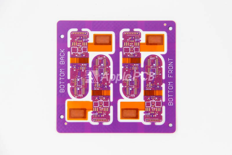
When designing the silkscreen, make sure that the character do not obscure pads, vias, RF tracks, or other important electrical connection locations that could affect the electrical function of the board and the quality of subsequent assembly. In general, it is best to maintain at least 6 mils of clearance between adjacent components.
2.PCB Silkscreen Text Size
The size of the silkscreen characters will directly affect the readability. Best font for pcb silkscreen should follow the rule of width/height=1:6 ratio, so as to ensure the high resolution of the silkscreen. pcb minimum silkscreen width is 4mil, if the PCB is too small it may not be able to print out, and if it is too big, it will be a waste of PCB space. According to the different copper thickness, the silkscreen width also changes.
| Base Copper(oz) | 0.5 | 1 | 2 |
| Minimum Silkscreen width (mil) | 4 | 5 | 6 |
| Silkscreen Height (mil) | 24 | 30 | 36 |
3.PCB Silkscreen Colors Selection
The silkscreen color should contrast with the solder mask of the PCB to improve readability. A common silkscreen color is white, as it provide good contrast on most solder mask color (e.g. green, black or blue). If your PCB solder mask color is light (e.g. white), it is recommended to use black silkscreen to ensure contrast. In short, the choice of silkscreen color should take into account the readability.
4.Multi-Pin Component Silkscreen
For multi-pin component (e.g. ICs), the silkscreen should show the number of all pins (e.g. 1, 2, 3, etc.). This help ensure that assemblers can clearly identify the location of each pin and prevent connection errors.
5.Polarity or Direction
For certain specific components, such as LEDs, electrolytic capacitors, diode pcb silkscreen, the polarity point or location of pin 1 must be clearly marked. This helps prevent circuit failures due to incorrect polarity.
3 Different PCB Silkscreen Printing Methods
ApplePCB offer three PCB silkscreen printing processes to choose from—each with its traits that we'll delve into regarding their pros and cons and production procedures.
Manual Screen Printing
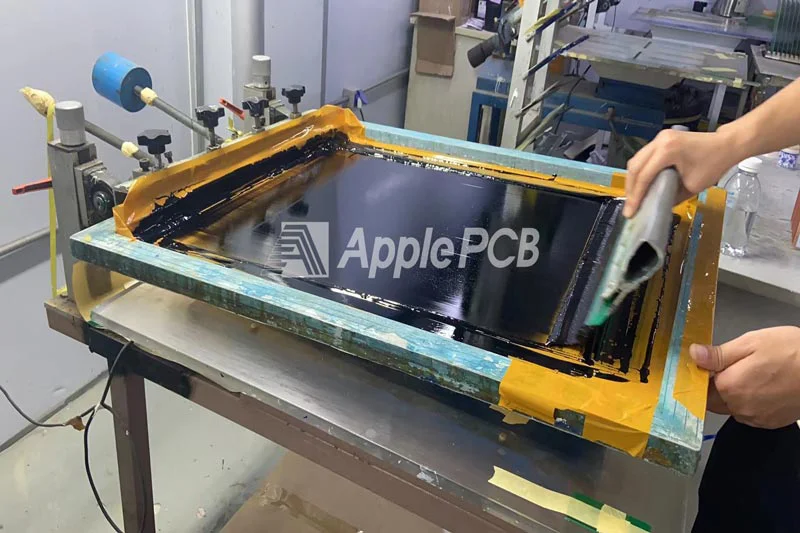
Manual silkscreen is the simplest and least expensive method of PCB silkscreen, and is especially suited to PCB designs with register tolerances of 0.005 inches or line widths greater than 0.007 inches. Despite its lower cost, manual silkscreen relies on operator experience and skill, so quality and accuracy often lack consistency. In addition, compared to automated printing methods, manual silkscreen has a slower production speed, is unsuitable for mass production, and struggles to meet the high-precision printing requirements of fine text and complex lines. Its process is as follows:
1.Creation of screen printing template: Create a template with the required pattern and text according to the design file. Template material is usually nylon to ensure its durability and reusability.
2.Align the stencil: Lets line up the stencil, with the PCB and apply ink on the surface.
3.Squeegee: Use the squeegee to push the printing ink evenly through the screen onto the PCB surface.
4.Baking and curing: After printing the ink, on the PCB place it in the baking oven(<48 degrees Celsius) for curing.
Liquid Photo Imaging
Liquid Photo Imaging (LPI) is an automated screen printing technology that is ideally suited for silkscreening line larger than 4 mil. However, it can only silkscreen white characters. And due to equipment and technology, it has long setup times and use more ink. The inks used in LPI are highly resistant to temperature change, humidity fluctuation, and chemical exposure, which explains its relatively high price.
However, despite the larger upfront investment the ability of LPI technology to significantly improve the quality and productivity of silkscreen printing makes this investment often considered a worthwhile option.The manufacturing process for LPI screen printing is somewhat similar to that of solder mask, with specific steps:
1.Apply photosensitive ink: Apply the ink evenly onto the surface of the PCB to make sure all area are adequately covered.
2.Placement of design film: A design photomask (usually a transparent film) is placed on the PCB surface coated with photosensitive ink to cover the area to be protected.
3.Ultraviolet exposure: The board is exposed to ultraviolet light. The part not covered by light mask will harden to form the desired print pattern.
4.Developing Process: A developing solution is used to clean off the unexposed areas, leaving the desired silkscreen design.
Direct Graphic Printing
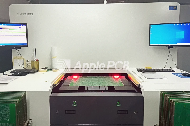
Direct Graphic Printing (DLP), also known as automated silkscreen, uses an inkjet printer to print design directly onto PCB, operating on a similar principle to the paper printers we use. Unlike manual silkscreen, it does not require traditional stencils, greatly simplifying the process steps. And it is fully automated, which also reduces human error. It therefore excels in speed and quality and is suitable for the quick turn of printed circuit boards.
Unlike the previous two, the DLP silkscreen process uses acrylic inks. Due to the nature of the ink and the process, DLP technology is not suitable for PCB that are less than 0.02 inches thick or silver-based, as this may result in blurred or unclear character. The DLP process step are as follow:
1.Prepare the digital file: Firstly create a file that includes the screen printing design you want to use.This file is typically made using CAD software. Includes all the text,symbols and patterns that will be printed.
2.Setting up the printer: Involve making sure that the PCB is correctly positioned alongside the printer. Then tweaking the printing setting of the device to match the specification of the design.
3.Spray Ink: Insert the PCB into the printer and start printing. The printer sprays the legend directly onto the PCB surface using acrylic ink according to the digital design file.
Manual Silkscreen vs DLP vs LPI
| Aspect | Manual Silkscreen | DLP | LPI | |
| Advantages | Precision | Moderate to High | Moderate to High | High |
| Resolution | Good | Good | Excellent | |
| Complex Designs | Limited | Limited | Well-suited | |
| High Detail | Limited | Limited | Yes | |
| Disadvantages | Cost | Moderate | Lower | Higher |
| Setup Time | Moderate | Shorter | Longer | |
| DFM | Design Complexity | Simplified | Simplified | Accommodated |
| Alignment Tolerances | Moderate | Critical | Critical | |
| Substrate Compatibility | Limited to flat surfaces | Broad range | Broad range | |
How to Determine PCB Silkscreen Cost?
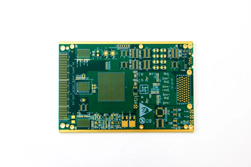
PCB print cost is typically 12-15% of the total PCB manufacturing cost. The choice of ink, the method of silkscreen, the complexity of the character design and the need for double-sided printing are all factor that affect the cost.
1.Ink Type
The ink formulation used by each manufacturer may vary, as specific additives are usually added to the ink to enhance its performance in terms of compatibility with the PCB substrate, adhesion, curing process, and resistance to acids and alkalis. Generally speaking, inks with better capabilities will also be relatively more expensive. To ensure the quality of silkscreen, ApplePCB always chooses globally recognized ink brands such as KSM and Taiyo, whose reliability has been widely recognized in the industry.
2.Silkscreen Color
The color of silkscreen is also a very important factor. Generally speaking common silkscreen colors (white, yellow and black) have lower cost, with white ink being the least expensive. While some uncommon colors such as blue, pink and purple will cause higher cost.
3.Silkscreen Processes
In addition to the ink itself, each silkscreen process require additional step. Manual screen printing requires the creation of stencils, the DLP process require more sophisticated equipment, and LPI require longer setup times, all of which add to the overall cost.
4.Silkscreen Designs
The design complexity, likes width, height, spacing, thickness, and position of the characters also affect the cost of silkscreen. The more complex the design, the more process step and adjustment are required, and the cost increase accordingly.
5.Double-sided Printing
If silkscreen is required on both sides of the PCB, the cost will almost double. Double-sided silkscreen mean increased ink usage, additional alignment and more production processes, which can significantly increase the overall cost.
Reducing PCB silkscreen costs can be achieved by optimizing material selection, simplifying design, and more. By sensibly controlling these factors, ApplePCB expect to reduce silkscreen costs by about 5%. If you are looking for ways to further optimize print pcb price, you can contact us for more professional advice and a detailed quote!
ApplePCB’s PCB Print Service
| Items | Competencies |
| Silkscreen Colour | White, Yellow, Black |
| Solder Silkscreen Brand | KSM-388 white/black Taiyo S-380W white ATA-5000 yellow |
| Silkscreen Line Width and Text Height | Line Width 5mil Text Height 27mil |
| Character Printer(Only White) | Serial, Bar Code, QR Code. |
| Silkscreen to Solder Pad Space | 6mil |
Final Thoughts
Through this article, it is easy to see that pcb silkscreen is a complicated process which can affect the overall quality of the PCB, so it is recommended that you look for an experienced and professional PCB manufacturer to help you with your silkscreen design. As a PCB board printing company in China with 15 years experience, ApplePCB specializes in providing one-stop PCB services from design, manufacturing to assembly. We can provide you with professional pcb silkscreen custom service, if you want to get a quote or learn more information, you can contact us through the lower right corner.
